|
|
|
| Enhanced PdSe2/Si heterojunction photodetector by Al2O3 layer |
Yi-fei HE1( ),De-ren YANG1,2,Xiao-dong PI1,2,*() ),De-ren YANG1,2,Xiao-dong PI1,2,*() |
1. School of Materials Science and Engineering, Zhejiang University, Hangzhou 310027, China
2. Hangzhou Global Scientific and Technological Innovation Center, Zhejiang University, Hangzhou 311200, China |
|
|
|
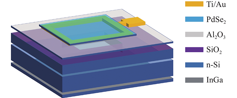
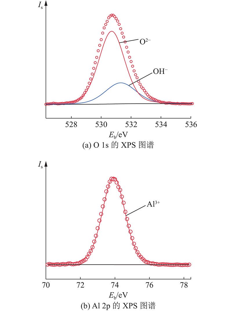
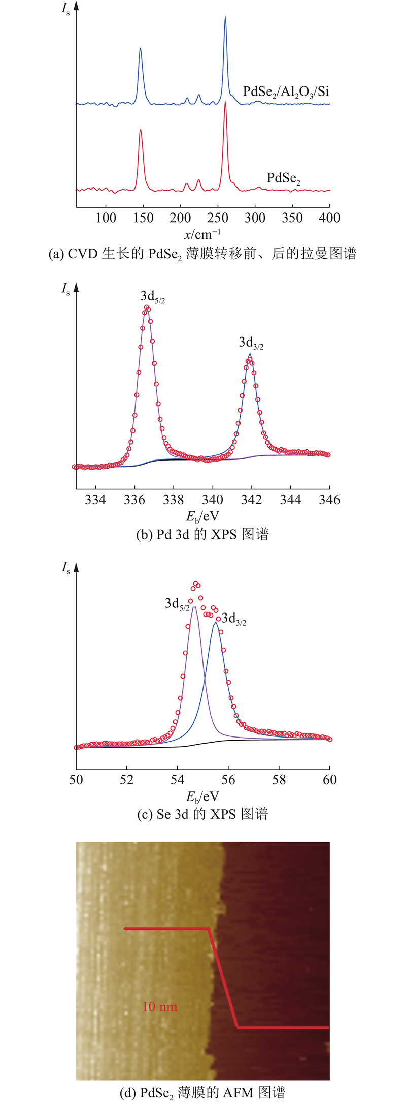
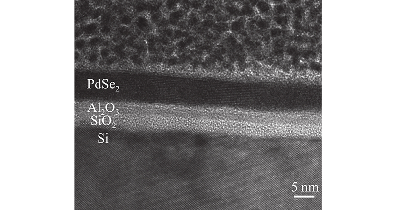
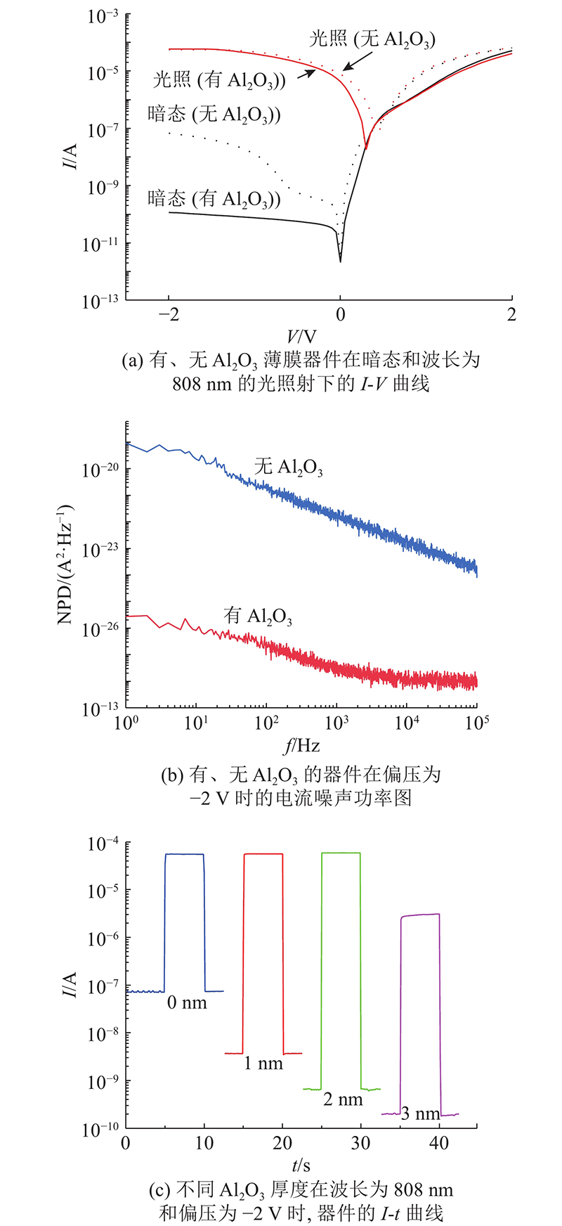
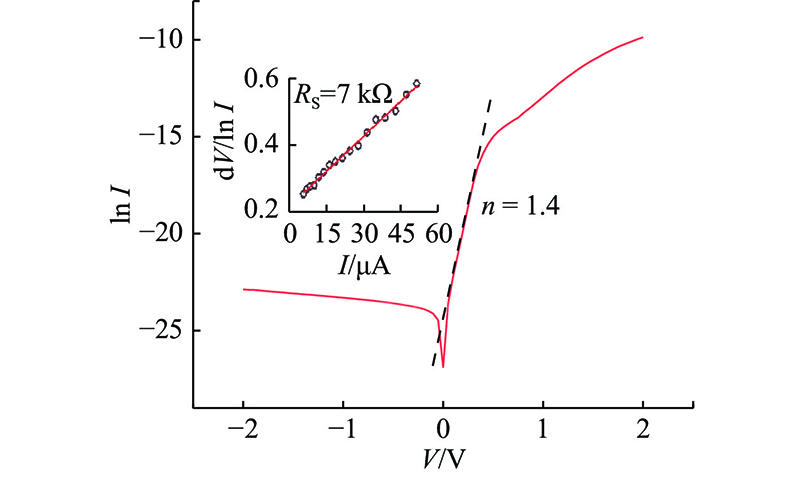
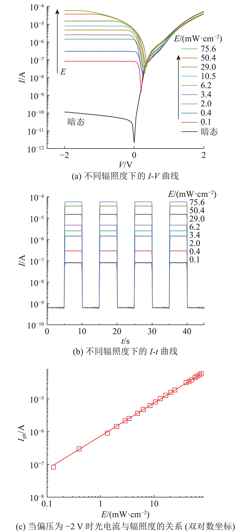
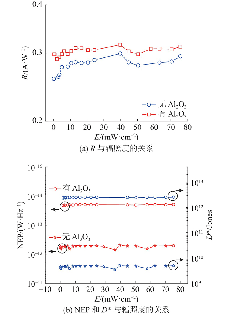
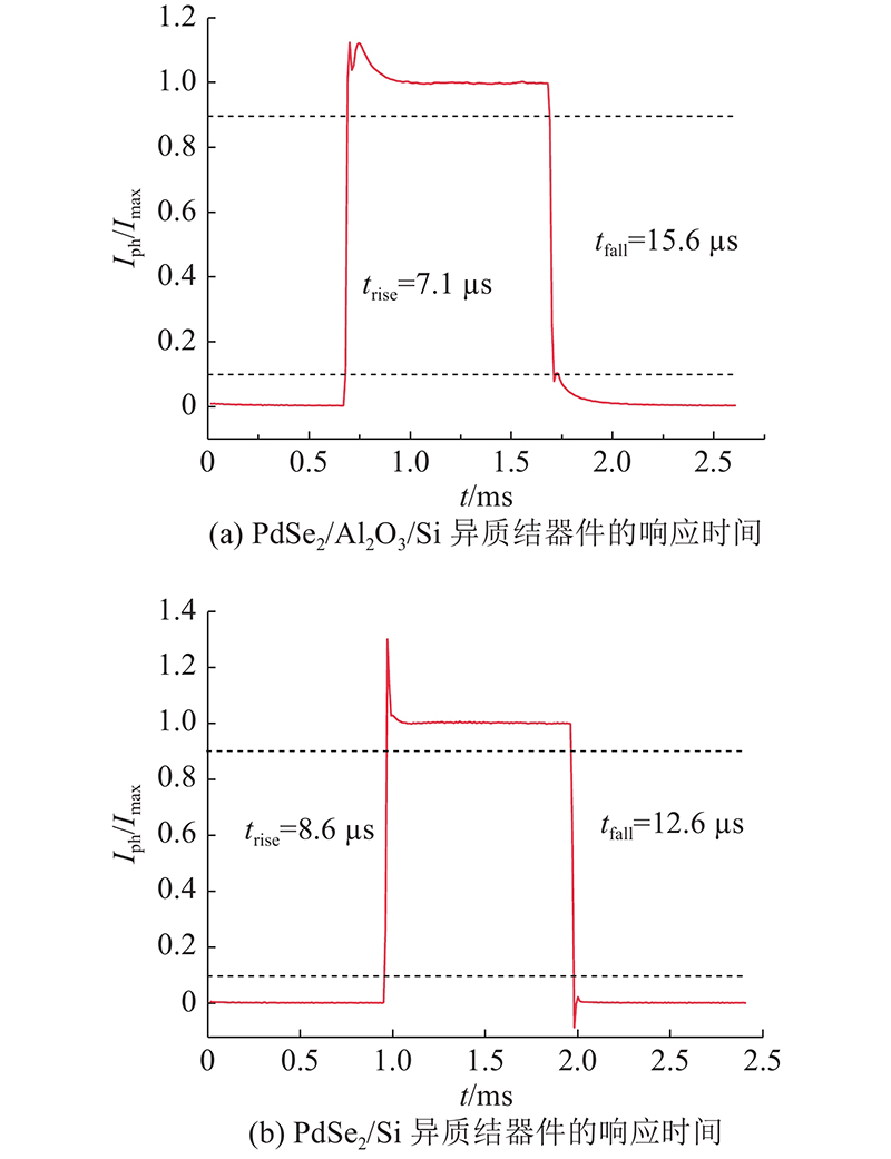
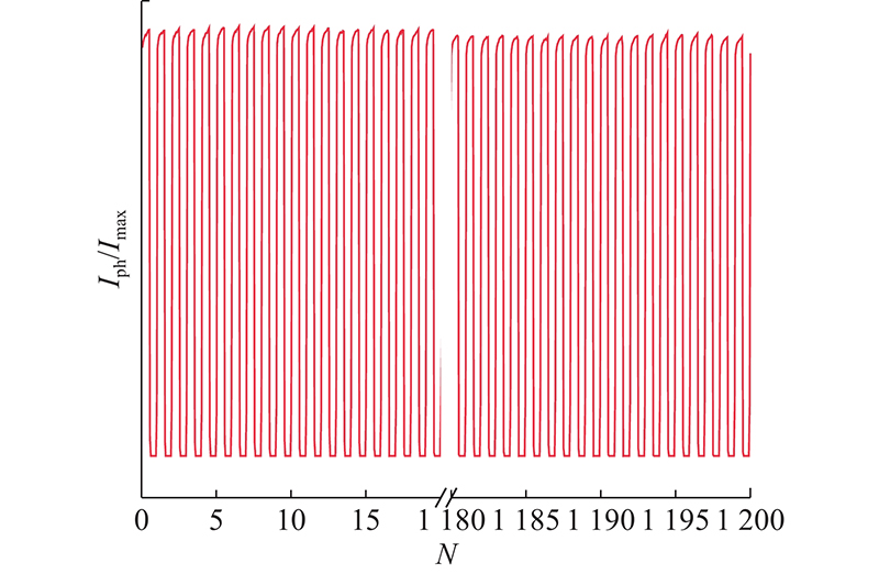
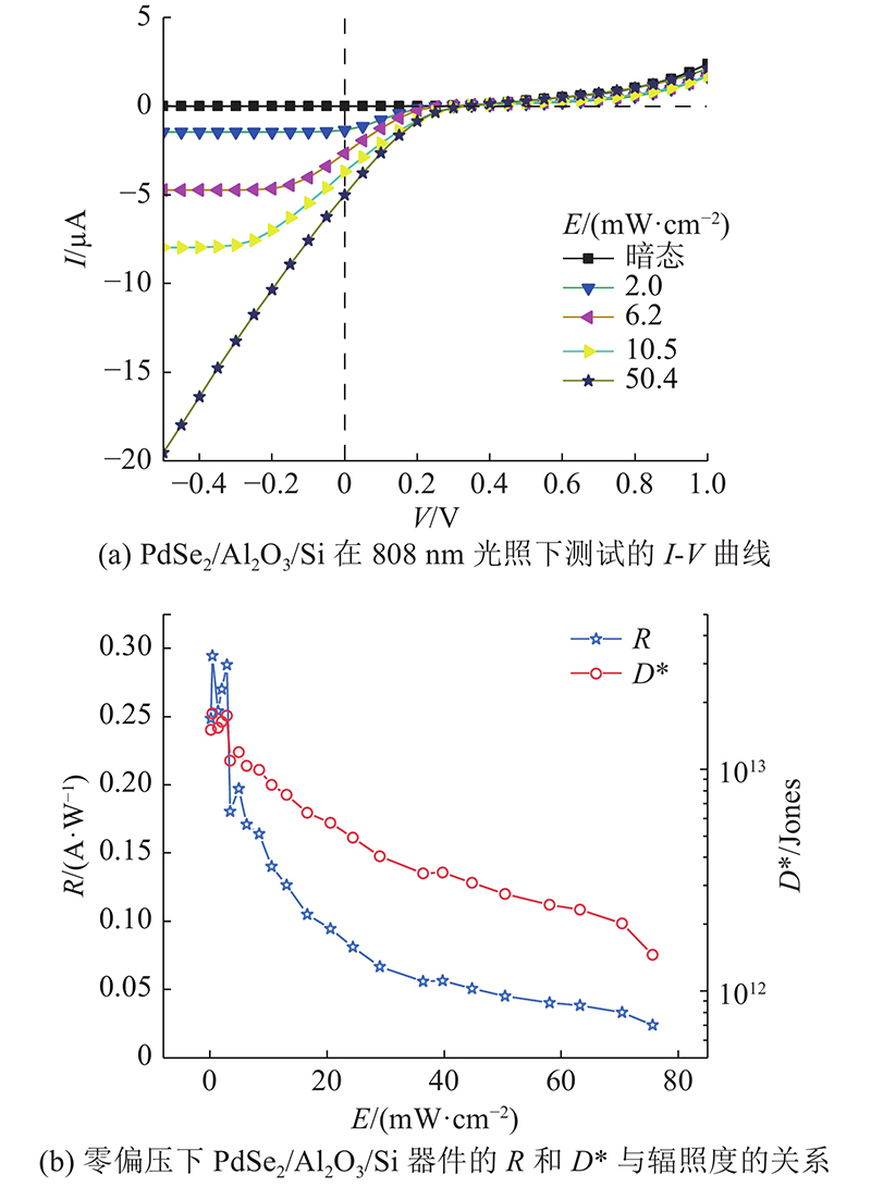
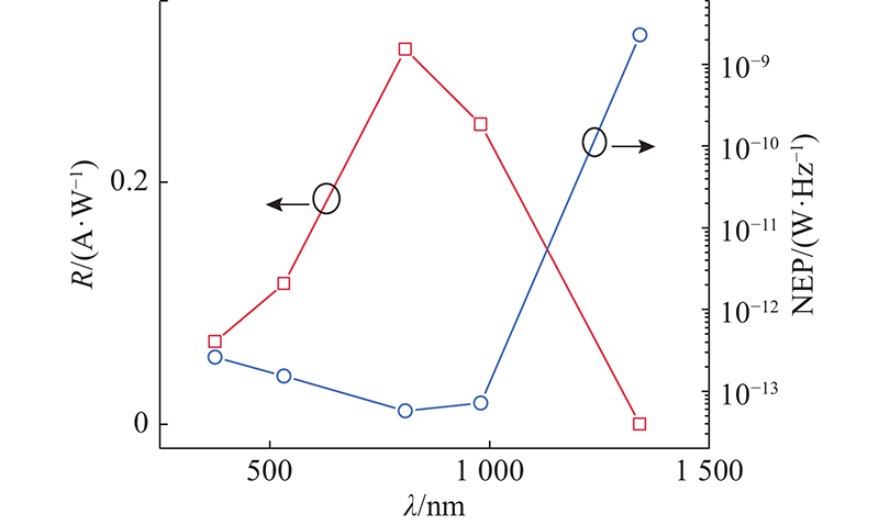
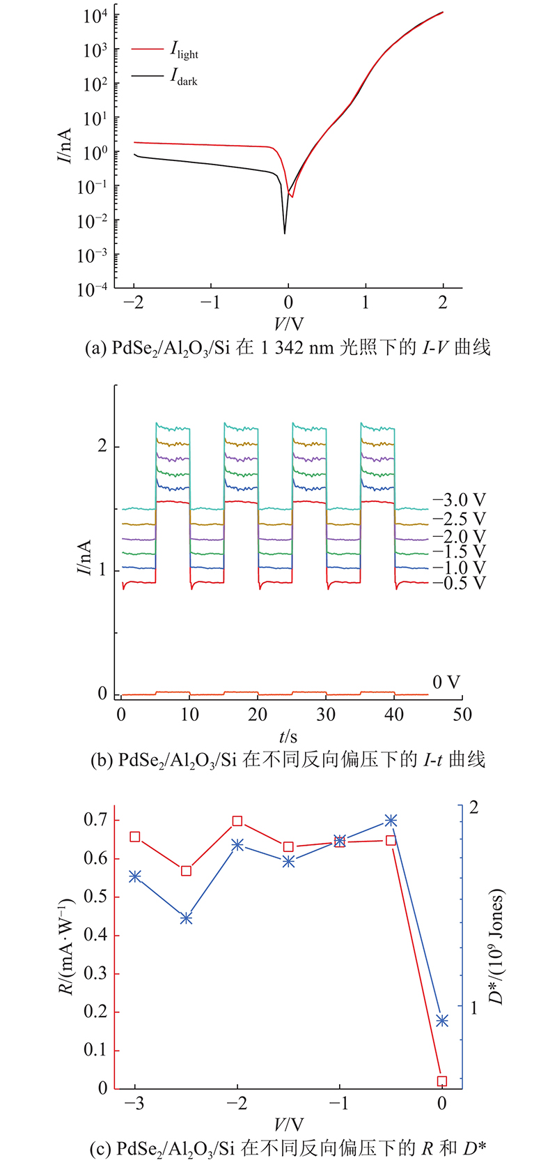
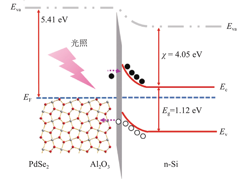
Abstract PdSe2/Al2O3/Si heterojunction device was fabricated by inserting Al2O3 tunneling layer grown by atomic layer deposition (ALD) in order to decrease the dark current. A fast and broadband photodetector was realized by optimizing the thickness of Al2O3. Results showed that the dark current of PdSe2/Al2O3/Si device was reduced by about 3 orders of magnitude compared with the device without Al2O3 layer under 808 nm illumination and ?2 V bias voltage. The photoresponsivity of the device was about 0.31 A/W and the corresponding specific detectivity was about 2.5×10 12 Jones. The device exhibited obvious self-driving effect without bias. The device still maintained a better photoresponse after 1 200 cycles of cyclic testing. The rise time and fall time of photoresponse were 7.1 μs and 15.6 μs, respectively. The introduction of Al2O3 tunneling layer between the two-dimensional layered semiconductor material and silicon can effectively reduce the dark current of the device and is beneficial to achieving high-performance silicon-based photodetectors.
|
|
Received: 08 April 2022
Published: 17 January 2023
|
|
|
| Fund: 国家重点研发计划资助项目(2017YFA0205700,2018YFB2200101) |
|
Corresponding Authors:
Xiao-dong PI
E-mail: yf_h@zju.edu.cn;xdpi@zju.edu.cn
|
氧化铝增强的PdSe2/Si异质结光电探测器
为了降低暗电流,通过原子层沉积(ALD)生长了一层氧化铝(Al2O3)隧穿层,制备了PdSe2/Al2O3/Si异质结光电探测器. 通过优化Al2O3层的厚度,使得该探测器实现了高速和宽光谱响应. 研究结果表明,在波长为808 nm的光照射和?2 V偏压下,所制备的光电探测器与未生长Al2O3的器件相比,暗电流降低了约3个数量级,器件的光响应度达到了约为0.31 A/W,对应的比探测率约为2.5×1012 Jones,器件在零偏压下表现出明显的自驱动效应. 经过循环测试1 200次后,器件保持良好的光响应. 器件响应的上升时间和下降时间分别为7.1和15.6 μs. 结果表明,在二维层状半导体材料与Si之间引入Al2O3隧穿层,可以有效地降低器件的暗电流,有利于高性能的Si基光电探测器的制备.
关键词:
硅,
二硒化钯,
异质结,
原子层沉积(ALD),
快速光响应,
隧穿光电探测器
|
|
| [1] |
AN X, LIU F, JUNG Y J, et al. Tunable graphene–silicon heterojunctions for ultrasensitive photodetection [J]. Nano Letters, 2013, 13 (3): 909-916.
|
|
|
| [2] |
ZENG L H, WANG M Z, HU H, et al Monolayer graphene/germanium schottky junction as high-performance self-driven infrared light photodetector[J]. ACS Applied Materials and Interfaces, 2013, 5 (19): 9362- 9366
doi: 10.1021/am4026505
|
|
|
| [3] |
ZHANG L, WANG B, ZHOU Y, et al. Synthesis techniques, optoelectronic properties, and broadband photodetection of thin-film black phosphorus [J]. Advanced Optical Materials, 2020, 8 (15): 2000045.
|
|
|
| [4] |
TAN S J R, ABDELWAHAB I, CHU L, et al. Quasi-monolayer black phosphorus with high mobility and air stability [J]. Advanced Materials, 2018, 30(6): 1704619.
|
|
|
| [5] |
WU D, GUO J, WANG C, et al Ultrabroadband and high-detectivity photodetector based on WS2/Ge heterojunction through defect engineering and interface passivation [J]. ACS Nano, 2021, 15 (6): 10119- 10129
doi: 10.1021/acsnano.1c02007
|
|
|
| [6] |
SONG Z, WANG Y, ZHU Y, et al. Targeted transfer of self-assembled cdse nanoplatelet film onto WS2 flakes to construct hybrid heterostructures [J]. Journal of Semiconductors, 2021, 42(8): 082901.
|
|
|
| [7] |
TIAN X, LIU Y Van der waals heterojunction ReSe2/WS2 polarization-resolved photodetector [J]. Journal of Semiconductors, 2021, 42 (3): 032001
doi: 10.1088/1674-4926/42/3/032001
|
|
|
| [8] |
TSAI D S, LIU K K, LIEN D H, et al Few-layer MoS2 with high broadband photogain and fast optical switching for use in harsh environments [J]. ACS Nano, 2013, 7 (5): 3905- 3911
doi: 10.1021/nn305301b
|
|
|
| [9] |
CHOI M S, QU D, LEE D, et al Lateral MoS2 p-n junction formed by chemical doping for use in high-performance optoelectronics [J]. ACS Nano, 2014, 8 (9): 9332- 9340
doi: 10.1021/nn503284n
|
|
|
| [10] |
CHEN Y Growth of a large, single-crystalline WS2 monolayer for high-performance photodetectors by chemical vapor deposition [J]. Micromachines, 2021, 12 (2): 2072
|
|
|
| [11] |
HAFEEZ M, GAN L, LI H, et al. Chemical vapor deposition synthesis of ultrathin hexagonal ReSe2 flakes for anisotropic raman property and optoelectronic application [J]. Advanced Materials, 2016, 28 (37): 8296-8301.
|
|
|
| [12] |
ZHANG E, JIN Y, YUAN X, et al ReS2-based field-effect transistors and photodetectors [J]. Advanced Functional Materials, 2015, 25 (26): 4076- 4082
doi: 10.1002/adfm.201500969
|
|
|
| [13] |
WANG Y, PANG J, CHENG Q, et al Applications of 2D-layered palladium diselenide and its van der waals heterostructures in electronics and optoelectronics[J]. Nano-Micro Letters, 2021, 13 (1): 143
doi: 10.1007/s40820-021-00660-0
|
|
|
| [14] |
ZENG L, WU D, JIE J, et al. Van der waals epitaxial growth of mosaic-like 2D platinum ditelluride layers for room-temperature mid-infrared photodetection up to 10.6 µm [J]. Advanced Materials, 2020, 32(52): 2004412.
|
|
|
| [15] |
DI BARTOLOMEO A, URBAN F, PELELLA A, et al Electron irradiation of multilayer PdSe2 field effect transistors [J]. Nanotechnology, 2020, 31 (37): 375204
doi: 10.1088/1361-6528/ab9472
|
|
|
| [16] |
LI G, YIN S, TAN C, et al. Fast photothermoelectric response in CVD-grown PdSe2 photodetectors with in-plane anisotropy [J]. Advanced Functional Materials, 2021, 31 (40): 2104787.
|
|
|
| [17] |
DI BARTOLOMEO A, PELELLA A, URBAN F, et al. Field emission in ultrathin PdSe2 back-gated transistors [J]. Advanced Electronic Materials, 2020, 6 (7): 2000094.
|
|
|
| [18] |
WU D, MO Z, HAN Y, et al Fabrication of 2D PdSe2/3D CdTe mixed-dimensional van der waals heterojunction for broadband infrared detection [J]. ACS Applied Materials and Interfaces, 2021, 13 (35): 41791- 41801
doi: 10.1021/acsami.1c11277
|
|
|
| [19] |
LU L S, CHEN G H, CHENG H Y, et al Layer-dependent and in-plane anisotropic properties of low-temperature synthesized few-layer PdSe2 single crystals [J]. ACS Nano, 2020, 14 (4): 4963- 4972
doi: 10.1021/acsnano.0c01139
|
|
|
| [20] |
VENKATESAN A, RATHI S, KIM Y, et al Few-layer PdSe2-based field-effect transistor for photodetector applications [J]. Materials Science in Semiconductor Processing, 2020, 115 (15): 105102
|
|
|
| [21] |
OYEDELE A D, YANG S, LIANG L, et al PdSe2: pentagonal two-dimensional layers with high air stability for electronics [J]. Journal of the American Chemical Society, 2017, 139 (40): 14090- 14097
doi: 10.1021/jacs.7b04865
|
|
|
| [22] |
LIANG Q J, WANG Q X, ZHANG Q, et al High-performance, room temperature, ultra-broadband photodetectors based on air-stable PdSe2[J]. Advanced Materials, 2019, 31 (24): 1807609
|
|
|
| [23] |
WU D, GUO J, DU J, et al Highly polarization-sensitive, broadband, self-powered photodetector based on graphene/PdSe2/germanium heterojunction [J]. ACS Nano, 2019, 13 (9): 9907- 9917
doi: 10.1021/acsnano.9b03994
|
|
|
| [24] |
WU D, XU M, ZENG L, et al In situ fabrication of PdSe2/GaN schottky junction for polarization-sensitive ultraviolet photodetection with high dichroic ratio [J]. ACS Nano, 2022, 16 (4): 5545- 5555
doi: 10.1021/acsnano.1c10181
|
|
|
| [25] |
WALMSLEY T S, ANDREWS K, WANG T, et al. Near-infrared optical transitions in PdSe2 phototransistors [J]. Nanoscale, 2019, 11 (30): 14410-14416.
|
|
|
| [26] |
ZENG L H, WU D, LIN S H, et al. Controlled synthesis of 2D palladium diselenide for sensitive photodetector applications [J]. Advanced Functional Materials, 2019, 29 (1): 1806878.
|
|
|
| [27] |
YIN J, LIU L, ZANG Y, et al Engineered tunneling layer with enhanced impact ionization for detection improvement in graphene/silicon heterojunction photodetectors[J]. Light: Science and Applications, 2021, 10 (1): 113
doi: 10.1038/s41377-021-00553-2
|
|
|
| [28] |
WANG B, ZHU Y, DONG J, et al Self-powered, superior high gain silicon-based near-infrared photosensing for low-power light communication[J]. Nano Energy, 2020, 70 (1): 104544
|
|
|
| [29] |
ZHAO Y, CHEN J Surface plasmon resonance bilayer graphene/Al2O3/GaAs schottky junction near-infrared photodetector [J]. Journal of Alloys and Compounds, 2022, 900 (1): 163439
|
|
|
| [30] |
WON U Y, LEE B H, KIM Y R, et al Efficient photovoltaic effect in graphene/h-BN/silicon heterostructure self-powered photodetector[J]. Nano Research, 2021, 14 (6): 1967- 1972
doi: 10.1007/s12274-020-2866-x
|
|
|
| [31] |
PAK Y, PARK W, MITRA S, et al. Enhanced performance of MoS2 photodetectors by inserting an ALD-processed TiO2 interlayer [J]. Small, 2018, 14 (5): 1703176.
|
|
|
| [32] |
ALSHEHRI A H, MISTRY K, NGUYEN V H, et al. Quantum-tunneling metal-insulator-metal diodes made by rapid atmospheric pressure chemical vapor deposition [J]. Advanced Functional Materials, 2019, 29 (7): 1805533.
|
|
|
| [33] |
WU D, JIA C, SHI F H, et al Mixed-dimensional PdSe2/SiNWA heterostructure based photovoltaic detectors for self-driven, broadband photodetection, infrared imaging and humidity sensing [J]. Journal of Materials Chemistry A, 2020, 8 (7): 3632- 3642
doi: 10.1039/C9TA13611H
|
|
|
| [34] |
VUL A Y, DIDEIKIN A T Photodetectors based on metal-tunnel insulator-semiconductor structures[J]. Sensors and Actuators A: Physical, 1993, 39 (1): 7- 18
doi: 10.1016/0924-4247(93)80175-G
|
|
|
| [35] |
KIM C, YOO T J, CHANG K E, et al Highly responsive near-infrared photodetector with low dark current using graphene/germanium schottky junction with Al2O3 interfacial layer [J]. Nanophotonics, 2021, 10 (5): 1573- 1579
doi: 10.1515/nanoph-2021-0002
|
|
|
| [36] |
DURMUŞ P, YıLDıRıM M Gaussian distribution of inhomogeneous barrier height in Au/n-Si (111) schottky barrier diodes at low temperatures[J]. Materials Science in Semiconductor Processing, 2014, 27 (1): 145- 149
|
|
|
| [37] |
YU T, WANG F, XU Y, et al Graphene coupled with silicon quantum dots for high-performance bulk-silicon-based schottky-junction photodetectors[J]. Advanced Materials, 2016, 28 (24): 4912- 4919
doi: 10.1002/adma.201506140
|
|
|
| [38] |
WANG L, JIE J, SHAO Z, et al MoS2/Si heterojunction with vertically standing layered structure for ultrafast, high-detectivity, self-driven visible-near infrared photodetectors [J]. Advanced Functional Materials, 2015, 25 (19): 2910- 2919
doi: 10.1002/adfm.201500216
|
|
|
| [39] |
刘恩科, 朱秉升, 罗晋生.半导体物理学[M]. 7版. 北京: 电子工业出版社, 2017: 188.
|
|
|
| [40] |
LEE S H, JEONG H, KIM D Y, et al Electroluminescence from h-bn by using Al2O3/h-BN multiple heterostructure [J]. Optics Express, 2019, 27 (14): 19692- 19701
doi: 10.1364/OE.27.019692
|
|
|
| [41] |
ZHU W J, TSO-PING M, TAMAGAWA T, et al Current transport in metal/hafnium oxide/silicon structure[J]. IEEE Electron Device Letters, 2002, 23 (2): 97- 99
doi: 10.1109/55.981318
|
|
|
|
Viewed |
|
|
|
Full text
|
|
|
|
|
Abstract
|
|
|
|
|
Cited |
|
|
|
|
| |
Shared |
|
|
|
|
| |
Discussed |
|
|
|
|