|
|
|
| New electrostatic discharge protection device for VBO high speed chip |
Ze-kun XU( ),Hong-yu SHEN,Tao HU,Xiang LI,Shu-rong DONG*() ),Hong-yu SHEN,Tao HU,Xiang LI,Shu-rong DONG*() |
| School of Microelectronics ESD Laboratory, Zhejiang University, Hangzhou 310027, China |
|
|
|
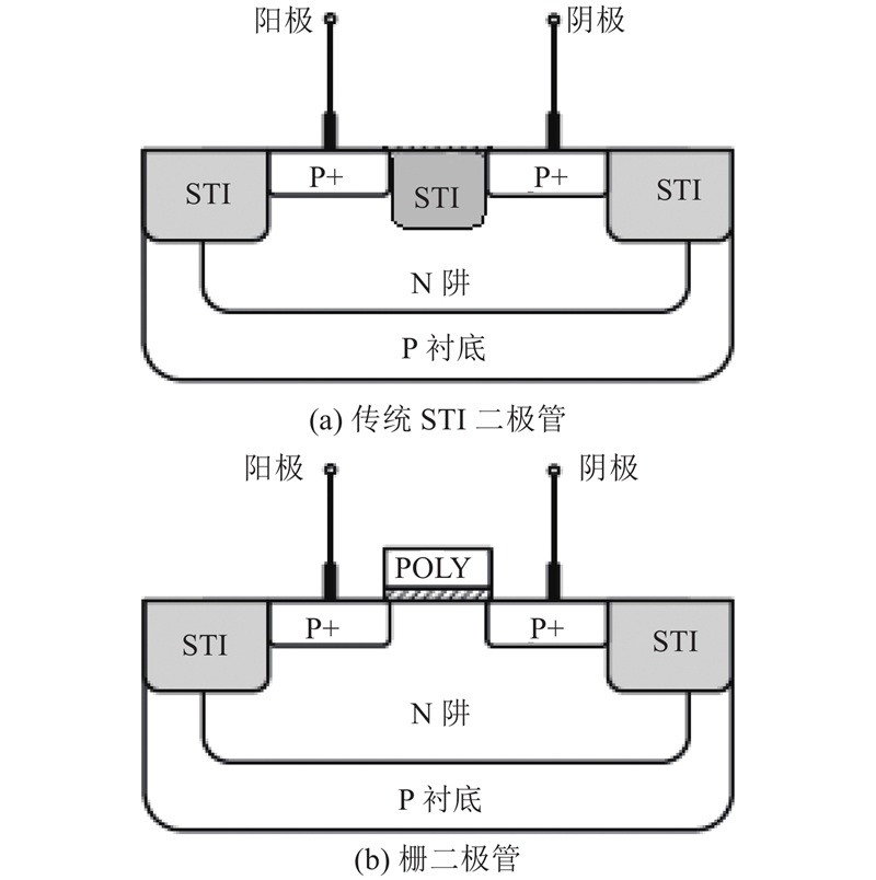
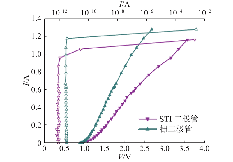
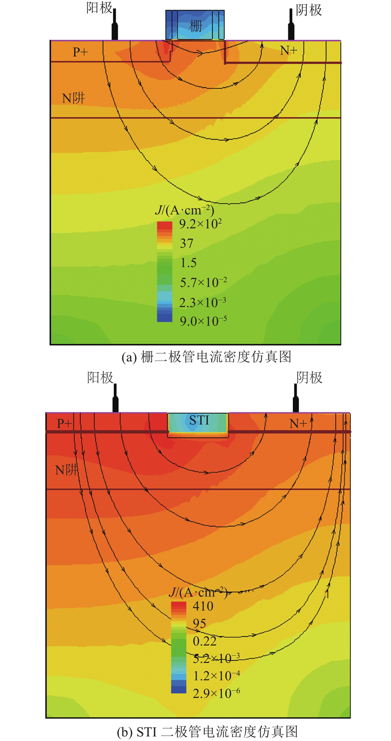
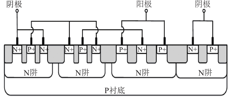
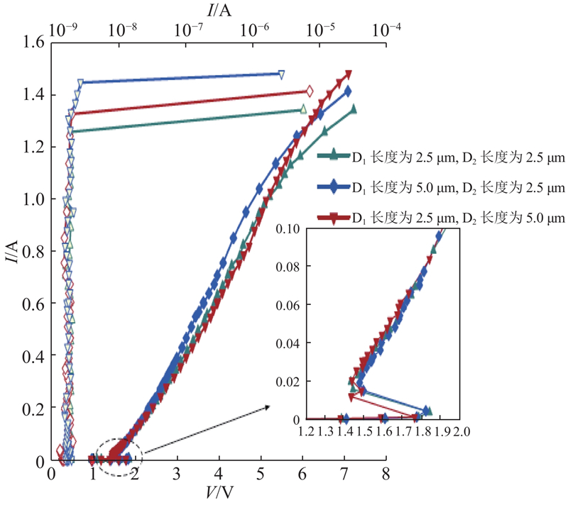
Abstract Two new electrostatic discharge (ESD) protection devices, gate diode and area-efficiency diode-trigger silicon controlled rectifier (SCR), were proposed in order to improve the performance of ESD protection devices on VBO interface circuit. Traditional diodes, gated diodes, and area-efficient SCR were fabricated based on SMIC 40 nm CMOS process and SMIC 28 nm PS CMOS process. The total current densities of those three structures were analyzed with the simulation of TCAD software. Ⅰ-Ⅴ characteristics of those ESD protection devices were measured by transmission line pulse (TLP) testing after tape-out. The gate diode's ESD robustness was 19.7 mA/μm, and on-resistance was 1.28 Ω with a 38.8% reduction compared to conventional diode. The trigger voltage of area-efficiency diode trigger SCR was 1.82 V and robustness of it was 48.1 mA/μm, which was a 174.8% improvement over conventional diode. The test results show that the performance of the gate diode and the ASCR is greatly improved compared to the conventional ESD device and is suitable to be the ESD device of VBO interface chip.
|
|
Received: 06 May 2018
Published: 28 March 2019
|
|
|
|
Corresponding Authors:
Shu-rong DONG
E-mail: xzkis1@163.com;dongshurong@zju.edu.cn
|
新型VBO接口芯片静电放电防护器件
为了改进VBO接口电路静电放电(ESD)防护器件性能,提出2种新的ESD防护器件:栅二极管与面积效率二极管触发可控硅整流器(SCR). 采用SMIC 40 nm CMOS工艺与SMIC 28 nm PS CMOS工艺制备传统二极管、栅二极管、面积效率SCR;通过半导体工艺及器件模拟工具(TCAD)进行仿真,分析电流密度;通过传输线脉冲测试(TLP)方法,测试不同结构ESD防护器件的Ⅰ-Ⅴ特性. 栅二极管的ESD鲁棒性为19.7 mA/μm,导通电阻为1.28 Ω,相较于传统二极管降低了38.8%. 面积效率二极管触发SCR触发电压为1.82 V,鲁棒性为48.1 mA/μm,相较于传统二极管提升了174.8%. 测试结果表明,栅二极管与ASCR和传统ESD器件相比,性能有极大的提升,适合用作VBO接口芯片的ESD防护.
关键词:
静电放电(ESD),
VBO,
可控硅整流器(SCR),
面积效率,
触发电压
|
|
| [1] |
MERRILL R, ISSAQ E. ESD design methodology [C] // Electrical Overstress/ Electrostatic Discharge Symposium. Lake Vista: IEEE, 1993: 233–237.
|
|
|
| [2] |
ABHHNAV V, CHATTERJEE A, SINHA D K, et al. Methodology for optimizing ESD protection for high speed LVDS based I/Os [C] // International Symposium on VlSI Design and Test. Hsinchu: IEEE, 2015: 1–5.
|
|
|
| [3] |
LIN C Y, KER M D, CHANG P H, et al. Study on the ESD-induced gate-oxide breakdown and the protection solution in 28 nm high-k metal-gate CMOS technology [C] // Nanotechnology Materials and Devices Conference. Toulouse: IEEE, 2016: 1–4.
|
|
|
| [4] |
曾杰. 新型集成电路ESD防护器件研究[D]. 浙江: 浙江大学, 2016.
ZENG Jie. Research of ESD protection device in new integrated circuit [D]. Zhejiang: Zhejiang University, 2016.
|
|
|
| [5] |
CHEN V, SALMAN A, BEEBE S, et al. SOI poly-defined diode for ESD protection in high speed I/Os [C] // Proceedings of IEEE International Reliability Physics Symposium. Piscataway: IEEE, 2006: 635–636.
|
|
|
| [6] |
LIN C Y, WU P H, KER M D Area-efficient and low-leakage diode string for on-chip ESD protection[J]. IEEE Transactions on Electron Devices, 2016, 63 (2): 531- 536
doi: 10.1109/TED.2015.2504493
|
|
|
| [7] |
LI C, WANG C, CHEN Q, et al. Characterization and analysis of diode-string ESD protection in 28 nm CMOS by VFTLP [C] // International Symposium on the Physical and Failure Analysis of Integrated Circuits. Chengdu: IEEE, 2017: 1–4.
|
|
|
| [8] |
YEH C T, KER M D, LIANG Y C Optimization on layout style of ESD protection diode for radio-frequency front-end and high-speed I/O interface circuits[J]. IEEE Transactions on Device and Materials Reliability, 2010, 10 (2): 238- 246
doi: 10.1109/TDMR.2010.2043433
|
|
|
| [9] |
CHATTERJEE A, POLGREEN T A low-voltage triggering SCR for on-chip ESD protection at output and input pads[J]. IEEE Electron Device Letters, 1991, 12 (1): 21- 22
doi: 10.1109/55.75685
|
|
|
| [10] |
KER M D, HSU K C. Complementary substrate- triggered SCR devices for on-chip ESD protection circuits [C] // ASIC/SOC Conference. New York: IEEE, 2002: 229–233.
|
|
|
| [11] |
GUO J, LIU J Z, TIAN R, et al. Novel diode-triggered silicon-controlled rectifier (DTSCR) for high-temperature low-voltage electrostatic discharge (ESD) applications [C] // IEEE International Nanoelectronics Conference. Chengdu: IEEE, 2016: 1–2.
|
|
|
| [12] |
LIU J, QIAN L, TIAN R, et al Self-triggered stacked silicon-controlled rectifier structure (STSSCR) for on-chip electrostatic discharge (ESD) protection[J]. Microelectronics Reliability, 2017, 71 (4): 1- 5
|
|
|
| [13] |
喻钊. FPGA全芯片ESD防护设计和优化[D]. 成都: 电子科技大学, 2012.
YU Zhao. FPGA full-chip ESD protection design and optimization [D]. Chengdu: University of Electronic Science and Technology of China, 2012.
|
|
|
| [14] |
MA F, HAN Y, DONG S R, et al Improved low-voltage-triggered SCR structure for RF-ESD protection[J]. IEEE Electron Device Letters, 2013, 34 (8): 1050- 1052
doi: 10.1109/LED.2013.2265411
|
|
|
|
Viewed |
|
|
|
Full text
|
|
|
|
|
Abstract
|
|
|
|
|
Cited |
|
|
|
|
| |
Shared |
|
|
|
|
| |
Discussed |
|
|
|
|