|
|
|
| Monolithic integrated resonant boost converter design |
Zi-heng LIU( ),Fan-yi MENG*(),Chen-fei WANG,Kai-xue MA ),Fan-yi MENG*(),Chen-fei WANG,Kai-xue MA |
| School of Microelectronics, Tianjin University, Tianjin 300072, China |
|
|
|
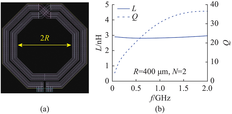
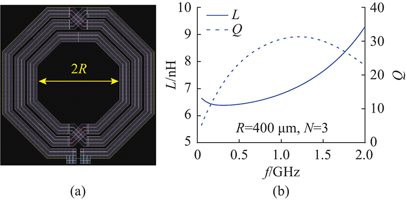
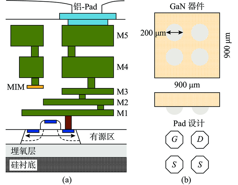
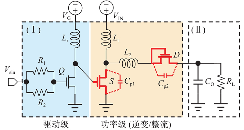
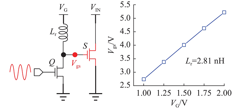
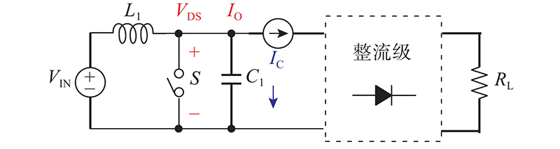
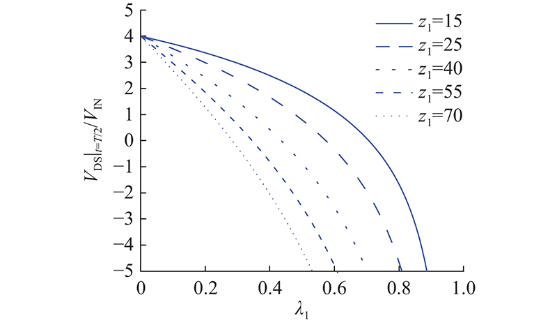
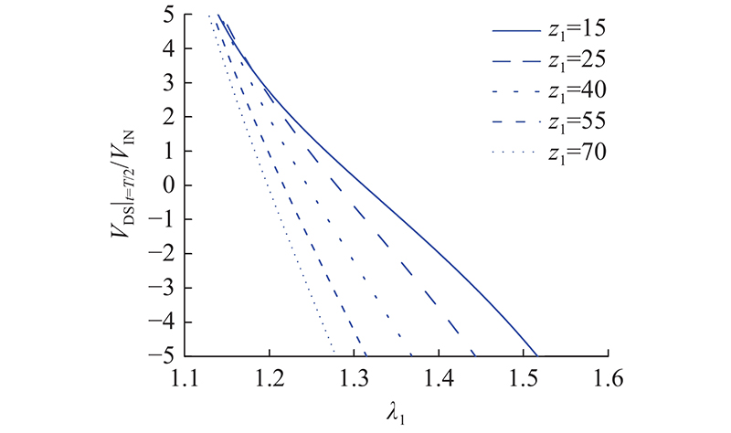
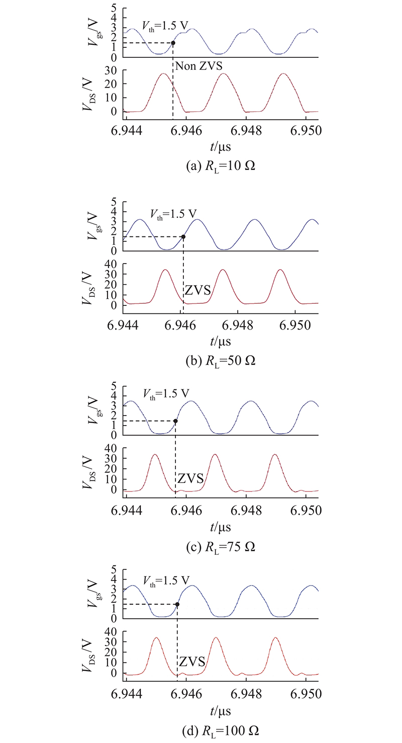
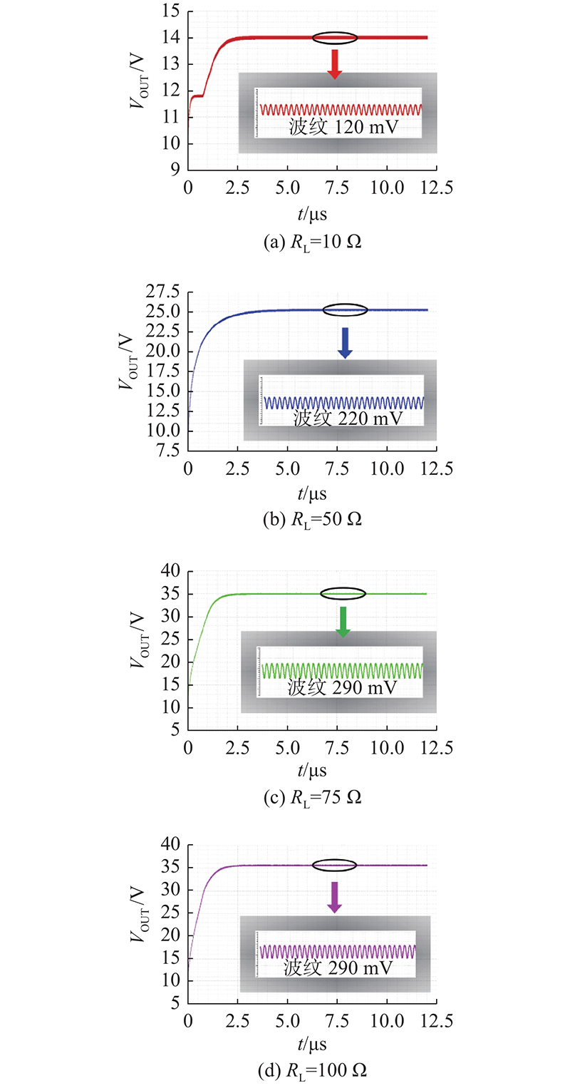
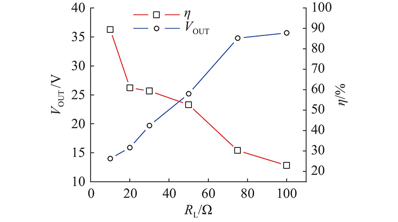
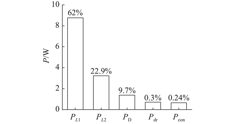
Abstract A three-dimensional integrated single-switch full-resonant boost converter was proposed based on silicon on insulator (SOI) process platform and gallium nitride (GaN) power transistors, in order to solve the problem of low power density of resonant power converters operating at high frequency. The switching frequency was 500 MHz. The main body of the converter adopted the derivative circuit structure of the traditional Class-E amplifier, i. e. parallel Class-E topology, and the gate driver adopted the single-switch resonant driving topology. The resonant inductance components in the converter were realized by the planar spiral inductor provided in the SOI process, the resonant capacitance components were realized by the Miller parasitic capacitance of the GaN power transistor, and the silicon-based chip and the GaN chip were connected by three-dimensional flip-chip technology. A detailed analysis was carried out around the design of circuit parameters, the realization of resonant components and the design of layout structure. Experimental results showed that when the input voltage was 12 V, the highest power density of the on-chip converter was 1.481W/mm2, the full-load efficiency was 60%, and the highest efficiency was 89%. This design provides a new idea for realizing power converter with high power density and high integration.
|
|
Received: 12 December 2021
Published: 31 May 2022
|
|
|
| Fund: 国家重点研发计划资助项目(2019YFB1803200) |
|
Corresponding Authors:
Fan-yi MENG
E-mail: zihengliu@tju.edu.cn;mengfanyi@tju.edu.cn
|
单片集成谐振式升压转换器设计
为了解决高频谐振功率转换器功率密度较低的问题,提出基于绝缘体上硅(SOI)工艺平台和氮化镓(GaN)功率晶体管的三维集成的单开关全谐振升压转换器,开关频率为500 MHz. 转换器主体采用传统Class-E放大器的衍生电路结构?并联式Class-E拓扑,栅极驱动器采用单管谐振式驱动拓扑. 转换器中的谐振电感元件采用SOI工艺中提供的平面螺旋电感实现,谐振电容元件采用GaN功率晶体管的米勒寄生电容实现,硅基芯片与GaN芯片通过三维倒装技术连接. 围绕电路参数设计、谐振元件的实现和版图结构设计进行详细分析. 实验结果显示,当输入电压为12 V时,片上转换器的最高功率密度为1.481 W/mm2,满载效率为60%,最高效率为89%. 本设计为实现高功率密度、高集成度的功率转换器提供了新思路.
关键词:
谐振式功率转换器,
三维集成,
电路设计,
功率密度,
转换效率
|
|
| [1] |
PILSOON C, UJWAL R, BOON C C, et al A fully integrated inductor-based GaN boost converter with self-generated switching signal for vehicular applications[J]. IEEE Transactions on Power Electronics, 2016, 31 (8): 5365- 5368
doi: 10.1109/TPEL.2016.2518183
|
|
|
| [2] |
JIANG J M, LIU X, KI W H, et al Circuit techniques for high efficiency fully-integrated switched-capacitor converters[J]. IEEE Transactions on Circuits and Systems II-Express Briefs, 2021, 68 (2): 556- 561
doi: 10.1109/TCSII.2020.3046514
|
|
|
| [3] |
谭平平, 桂成东, 姜立铭, 等 基于GaN器件的固态射频源应用研究[J]. 电源学报, 2020, 18 (4): 116- 122
TAN Ping-ping, GUI Cheng-dong, JIANG Li-ming, et al Research on applications of solid-state RF power supply based on GaN devices[J]. Journal of Power Supply, 2020, 18 (4): 116- 122
|
|
|
| [4] |
WANG Y J, LI F, QIU Y P, et al A single-stage LED driver based on flyback and modified Class-E resonant converters with low-voltage stress[J]. IEEE Transactions on Industrial Electronics, 2019, 66 (11): 8463- 8473
doi: 10.1109/TIE.2018.2890502
|
|
|
| [5] |
BURKHART J M, ROMAN K, PERREAULT D J Design methodology for a very high frequency resonant boost converter[J]. IEEE Transactions on Power Electronics, 2013, 28 (4): 1929- 1937
doi: 10.1109/TPEL.2012.2202128
|
|
|
| [6] |
LI Y, RUAN X B, ZHANG L, et al Variable switching frequency ON-OFF control for Class-E DC-DC converter[J]. IEEE Transactions on Power Electronics, 2019, 34 (9): 8859- 8870
doi: 10.1109/TPEL.2018.2888926
|
|
|
| [7] |
LEE K H, EUIHOON C, HAN Y S, et al A family of high frequency single-switch DC-DC converters with low switch voltage stress based on impedance networks[J]. IEEE Transactions on Power Electronics, 2017, 32 (4): 2913- 2924
doi: 10.1109/TPEL.2016.2580154
|
|
|
| [8] |
KERUI L, TAN S C, ADRIAN I, et al. DC-shifted harmonics-boosted resonant DC-DC converter with high-step-up conversion radio with ZVS over the full load range [C]// Applied Power Electronics Conference and Exposition (APEC). New Orleans: IEEE, 2019: 1307-1312.
|
|
|
| [9] |
ALESSANDRO N, GABRIELE A, GIORGIO C, et al. A 1.25 GHz fully integrated DC-DC converter using electromagnetically coupled Class-D LC oscillators [C]// 2021 IEEE International Solid-State Circuits Conference: Digest of Technical Papers. San Francisco: IEEE, 2021: 260-262.
|
|
|
| [10] |
AMIN S S, MERCIER P P A fully integrated Li-ion-compatible hybrid four-level DC-DC converter in 28-nm FDSOI[J]. Journal of Soild-State Circuits, 2019, 54 (3): 720- 732
doi: 10.1109/JSSC.2018.2880183
|
|
|
| [11] |
RENZ P, KAUFMANN M, LUEDERS M. A fully integrated 85%-peak-efficiency hybrid multi ratio resonant DC-DC converter with 3.0 V-to-4.5 V input and 500 μA-to-120 mA load range [C]// 2019 IEEE International Solid-State Circuits Conference: Digest of Technical Papers. San Francisco: IEEE, 2019: 156-158.
|
|
|
| [12] |
JIA T, GU Y A fully integrated buck regulator with 2-GHz resonant switching for low-power applications[J]. IEEE Journal of Solid-State Circuits, 2018, 53 (9): 2663- 2674
doi: 10.1109/JSSC.2018.2840513
|
|
|
| [13] |
MEYER C D, BEDAIR S S, MORGAN B C, et al. High-inductance-density, air-core, power inductors, and transformers designed for operation at 100-500 MHz [J] IEEE Transactions on Magnetics, 2010, 46(6): 2236-2239.
|
|
|
| [14] |
LIU S K, ZHU L, FREDERIC A, et al Physical models of planar spiral inductor integrated on the high-resistivity and trap-rich silicon-on-insulator substrates[J]. IEEE Transactions on Electron Devices, 2017, 64 (7): 2775- 2781
doi: 10.1109/TED.2017.2700022
|
|
|
| [15] |
LIU M J, SHAWNS H H A miniature 300-MHz resonant DC-DC converter with GaN and CMOS integrated in IPD technology[J]. IEEE Transactions on Power Electronics, 2018, 33 (11): 9656- 9668
doi: 10.1109/TPEL.2017.2788946
|
|
|
| [16] |
EYAL A, DANIEL P, KEVIN T, et al Hybrid CMOS/GaN 40-MHz maximum 20-V input DC-DC multiphase buck converter[J]. IEEE Journal of Solid-State Circuits, 2017, 52 (6): 1618- 1627
doi: 10.1109/JSSC.2017.2672986
|
|
|
| [17] |
MENG F Y, DON D, LIU B, et al Heterogeneous integration of GaN and BCD technologies and its applications to high conversion-ratio DC-DC boost converter IC[J]. IEEE Transactions on Power Electronics, 2019, 34 (3): 1993- 1996
doi: 10.1109/TPEL.2018.2859419
|
|
|
| [18] |
EPC2036-enhancement mode power transistor, EPC2036 datasheet. [EB/OL]. [2021-12-01]. https://epc-co.com/epc/Portals/0/epc/documents/datasheets/EPC2036_datasheet.pdf.
|
|
|
| [19] |
MCLAUGHLIN P H, XIA Z, STAUTH J T. A fully integrated resonant switched-capacitor converter with 85.5% efficiency at 0.47 W using on-chip dual-phase merged-LC resonator [C]// 2020 IEEE International Solid-State Circuits Conference: Digest of Technical Papers. San Francisco: IEEE, 2020: 192-194.
|
|
|
|
Viewed |
|
|
|
Full text
|
|
|
|
|
Abstract
|
|
|
|
|
Cited |
|
|
|
|
| |
Shared |
|
|
|
|
| |
Discussed |
|
|
|
|