|
|
|
| Design of high-speed driving control circuit for integrated silicon photonic switch matrix |
Yiyuan ZHANG1( ),Yating WU1,Guangcan MI2,Ying HUANG1,Tao CHU1,*() ),Yating WU1,Guangcan MI2,Ying HUANG1,Tao CHU1,*() |
1. College of Information Science and Electronic Engineering, Zhejiang University, Hangzhou 310027, China
2. Huawei Technologies Limited Company, Dongguan 523145, China |
|
|
|
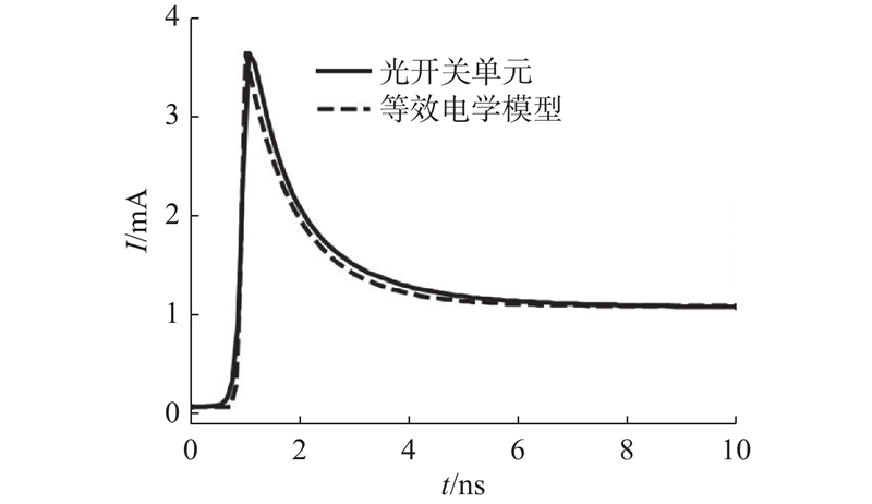
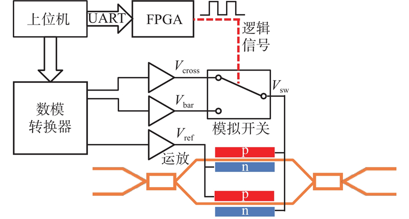
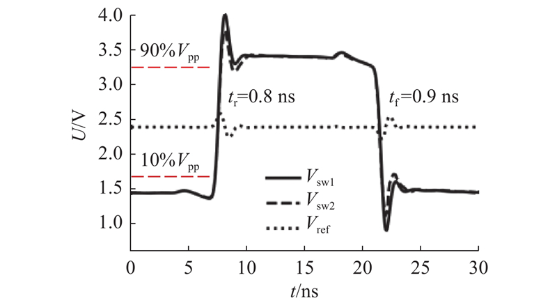
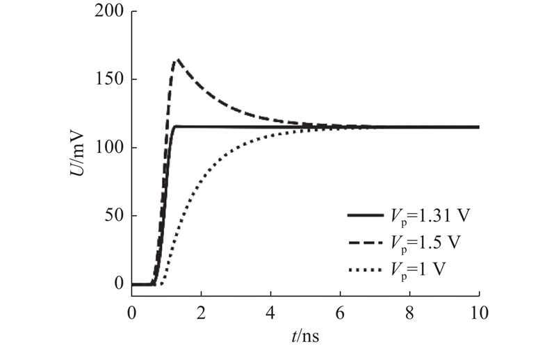
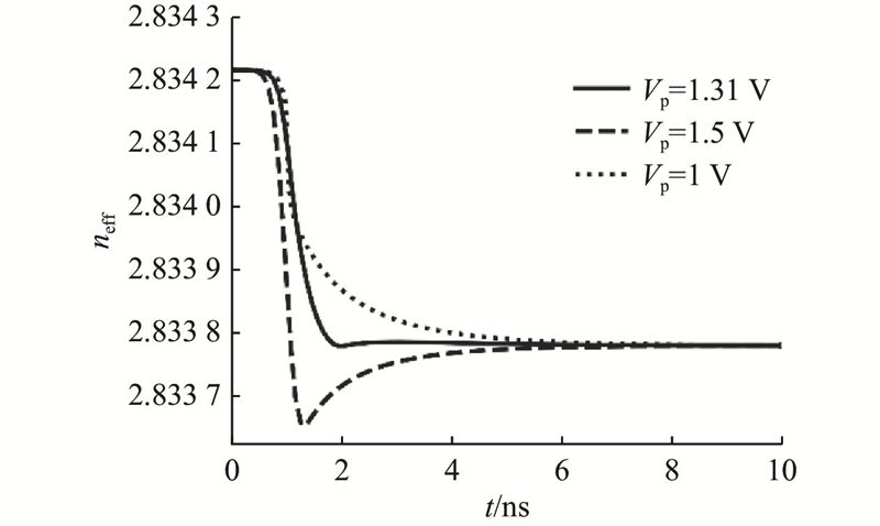
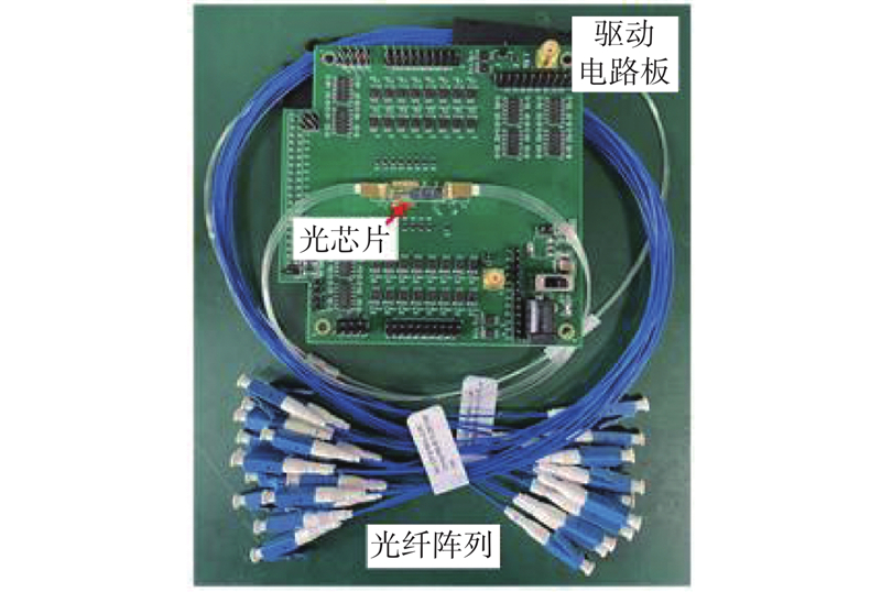
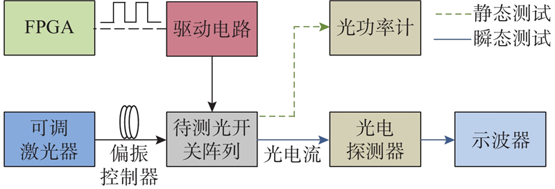
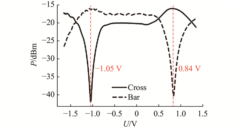
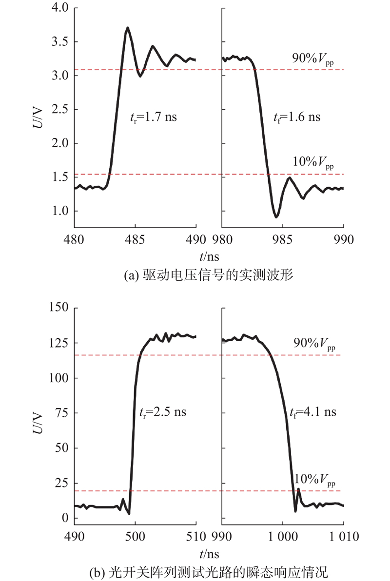
Abstract An equivalent electrical model was proposed for simulating the transient responses of a photonic switch cell by analyzing its physical structure. A high-speed driving control circuit was designed for a photonic switch matrix based on the model, and the effect of voltage spikes on the transient response of photonic switch cell was analyzed by simulation. The test results show that the rise/fall time of the signal supplied by the driving circuit are 1.7/1.6 ns, which meets the requirements for nanosecond-level switching of high-speed photonic switches. The switching time of the photonic switch matrix reaches 2.1?5.9 ns with the assistance of the driving control circuits, realizing a high-speed optical switching system.
|
|
Received: 23 May 2023
Published: 23 January 2024
|
|
|
| Fund: 国家自然科学基金资助项目(62035001) |
|
Corresponding Authors:
Tao CHU
E-mail: zhang_yiyuan@zju.edu.cn;chutao@zju.edu.cn
|
硅基集成光开关阵列的高速驱动控制电路设计
通过分析光开关单元的物理结构,提出等效电学模型,用于模拟光开关单元的瞬态响应. 基于该模型,针对光开关阵列设计高速驱动控制电路,结合仿真探究电压尖峰对光开关单元瞬态响应的影响. 系统测试结果表明,驱动电路施加的电压信号的上升/下降时间为1.7/1.6 ns,能够满足高速光开关纳秒级切换速度的需求. 在该驱动电路的配合下,光开关阵列的切换时间为2.1~5.9 ns,实现了较先进的高速光交换系统.
关键词:
光通信,
光互连,
硅基光子学,
硅基光开关,
驱动控制电路
|
|
| [1] |
CHU T, QIAO L, TANG W. High-speed 8×8 electro-optic switch matrix based on silicon PIN structure waveguides [C]// IEEE 12th International Conference on Group IV Photonics. Vancouver: IEEE, 2015: 123-124.
|
|
|
| [2] |
SIEW S Y, LI B, GAO F, et al Review of silicon photonics technology and platform development[J]. Journal of Lightwave Technology, 2021, 39 (13): 4374- 4389
doi: 10.1109/JLT.2021.3066203
|
|
|
| [3] |
WANG Y, WANG X, YUAN J, et al Monolithic III-nitride photonic circuit towards on-chip optical interconnection[J]. Applied Physics Express, 2018, 11 (12): 122201
|
|
|
| [4] |
BIBERMAN A, BERGMAN K Optical interconnection networks for high-performance computing systems[J]. Reports on Progress in Physics, 2012, 75 (4): 046402
|
|
|
| [5] |
XUE X, CALABRETTA N Nanosecond optical switching and control system for data center networks[J]. Nature Communications, 2022, 13 (1): 2257
|
|
|
| [6] |
HU G, QI Z, YUN B, et al High performance ridge type PLZT optical switch with offset upper electrode[J]. IEEE Photonics Technology Letters, 2015, 27 (21): 2257- 2259
|
|
|
| [7] |
QIAO L, TANG W, CHU T. Ultra-large-scale silicon optical switches [C]// IEEE 13th International Conference on Group IV Photonics. Shanghai: IEEE, 2016: 1-2.
|
|
|
| [8] |
SUZUKI K, KONOIKE R, SUDA S, et al. Low-loss, low-crosstalk, and large-scale silicon photonics switch [C]// Optical Fiber Communications Conference and Exhibition. San Diego: OSA, 2019: 1-3.
|
|
|
| [9] |
MORI Y, SATO K-I. Large-scale optical switch architectures for intra-datacentre networks [C]// European Conference on Optical Communications. Belgium: IEEE, 2020: 1-4.
|
|
|
| [10] |
SEOK T J, QUACK N, HAN S, et al Large-scale broadband digital silicon photonic switches with vertical adiabatic couplers[J]. Optica, 2016, 3 (1): 64- 70
|
|
|
| [11] |
ASSEFA S, SHANK S, GREEN W, et al. A 90nm CMOS integrated nano-photonics technology for 25Gbps WDM optical communications applications [C]// International Electron Devices Meeting. San Francisco: IEEE, 2012, 33(8): 1-3.
|
|
|
| [12] |
LEE B G, RYLYAKOV A V, GREEN W M J, et al Monolithic silicon integration of scaled photonic switch fabrics, CMOS logic, and device driver circuits[J]. Journal of Lightwave Technology, 2014, 32 (4): 743- 751
|
|
|
| [13] |
DUPUIS N, PROESEL J E, AINSPAN H, et al Nanosecond photonic switch architectures demonstrated in an all-digital monolithic platform[J]. Optics Letters, 2019, 44 (15): 3610- 3612
|
|
|
| [14] |
LEE B G, GREEN W M J, RYLYAKOV A V, et al. Monolithically integrated photonic switches driven by digital CMOS [C]// Conference on Lasers and Electro-Optics. Munich: OSA, 2013: 1-2.
|
|
|
| [15] |
JIANG J, GOODWILL D J, DUMAIS P, et al. 16x16 silicon photonic switch with nanosecond switch time and low-crosstalk architecture [C]// 45th European Conference on Optical Communication. Dublin: IEEE, 2019: 1-4.
|
|
|
| [16] |
BACHMANN M, BESSE P A, MELCHIOR H General self-imaging properties in N×N multimode interference couplers including phase relations[J]. Applied Optics, 1994, 33 (18): 3905- 3911
|
|
|
| [17] |
BABA T, AKIYAMA S, IMAI M, et al. 25-Gbps operation of silicon p-i-n Mach-Zehnder optical modulator with 100-μm-long phase shifter [C]// Conference on Lasers and Electro-Optics. Tokyo: IEEE, 2012: 1-2.
|
|
|
| [18] |
BABA T, AKIYAMA S, IMAI M, et al 25-Gb/s broadband silicon modulator with 0.31-V·cm VπL based on forward-biased PIN diodes embedded with passive equalizer[J]. Optics Express, 2015, 23 (26): 32950- 32960
|
|
|
| [19] |
SOREF R, BENNETT B Electrooptical effects in silicon[J]. IEEE Journal of Quantum Electronics, 1987, 23 (1): 123- 129
|
|
|
| [20] |
LIRA H L R, MANIPATRUNI S, LIPSON M Broadband hitless silicon electro-optic switch for on-chip optical networks[J]. Optics Express, 2009, 17 (25): 22271- 22280
|
|
|
| [21] |
QIAO L, TANG W, CHU T 32×32 silicon electro-optic switch with built-in monitors and balanced-status units[J]. Scientific Reports, 2017, 7 (1): 42306
|
|
|
| [22] |
AKIYAMA S, IMAI M, BABA T, et al Compact PIN-diode-based silicon modulator using side-wall grating waveguide[J]. IEEE Journal of Selected Topics in Quantum Electronics, 2013, 19 (6): 74- 84
|
|
|
| [23] |
KAMATH B Y T, MEYER R G, GRAY P R Relationship between frequency response and settling time of operational amplifiers[J]. IEEE Journal of Solid-State Circuits, 1974, 9 (6): 347- 352
|
|
|
|
Viewed |
|
|
|
Full text
|
|
|
|
|
Abstract
|
|
|
|
|
Cited |
|
|
|
|
| |
Shared |
|
|
|
|
| |
Discussed |
|
|
|
|