|
|
|
| Design of low power differential multiplexing beamformer |
Lin-nan LI( ),Wei ZHANG*(),Yan-jie DANG,Tai-an LI ),Wei ZHANG*(),Yan-jie DANG,Tai-an LI |
| College of Microelectronic, Tianjin University, Tianjin 300072, China |
|
|
|
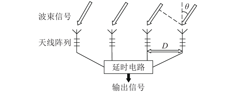
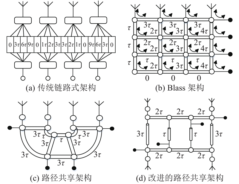
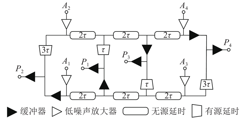
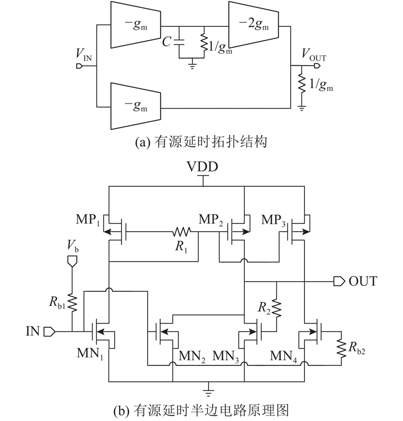
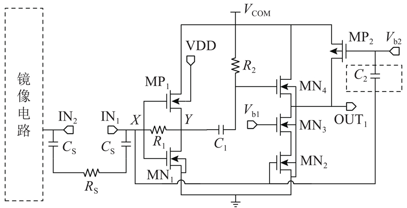
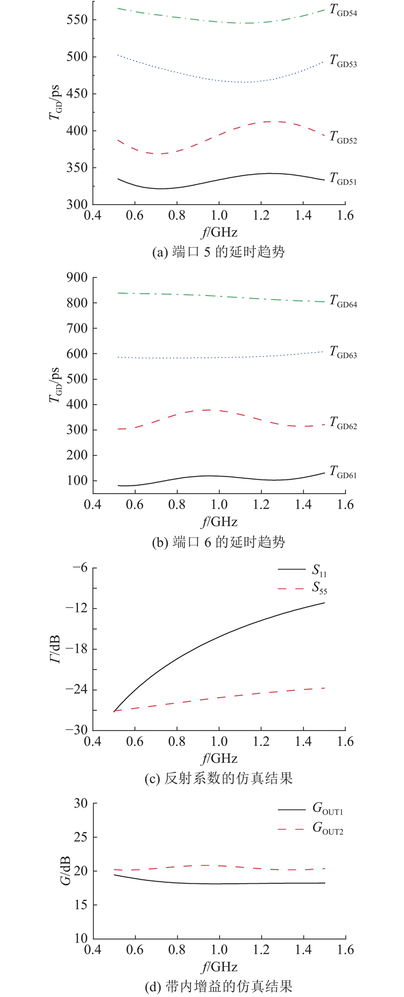
Abstract A new differential beamformer architecture was proposed to solve the problems of high power consumption and large scale of the traditional multiplexing network architecture, in order to make direct connection between beamformer and differential feed antennas, suppress noise and interference. The differential active delay units were used to replace the passive delay units and buffers on one-way path in the traditional architecture, and combined with the differential passive delay units on two-way path to form the fixed delay time differences among different paths. Based on HHNEC 0.18 μm CMOS technology, a four-input-four-output beamformer was designed to verify the proposed architecture. Simulation showed that in the 0.5—1.5 GHz bandwidth, the resolution of the delay network was 80 ps, the maximum delay value was 720 ps, the delay variation root mean square value was 29.7 ps, the output reflection coefficient of the circuit was lower than –23 dB, the input reflection coefficient was lower than ?10 dB, the in-band synthesis gain was 18—21 dB, the layout area was 2.96 mm × 3.22 mm, and the total power consumption at 1.8 V supply voltage was 303 mW. Experimental results show that the proposed structure has the advantages of high accuracy, moderate scale, low power consumption and low complexity.
|
|
Received: 19 February 2020
Published: 25 April 2021
|
|
|
| Fund: 国家重点研发计划资助项目(2016YFE0100400) |
|
Corresponding Authors:
Wei ZHANG
E-mail: lilinnan@tju.edu.cn;tjuzhangwei@tju.edu.cn
|
低功耗差分复用波束合成器的设计
为了实现波束合成器与差分馈电天线的直接连接,抑制噪声与干扰,针对传统复用网络架构的高功耗、大面积问题,提出新型差分波束合成架构. 采用差分有源延时单元代替传统架构单向通路上的无源延时单元和缓冲器,与双向通路上的差分无源延时单元结合,形成不同通路之间的固定延时差. 基于 HHNEC 0.18 μm CMOS 工艺,设计四输入四输出的波束合成器对所提架构进行验证. 仿真结果表明,在0.5~1.5 GHz带宽内,延时网络的分辨率为80 ps,最大延时值为720 ps,延时浮动均方根值为29.7 ps,电路的输出反射系数低于?23 dB,输入反射系数低于?10 dB,带内增益为18~21 dB,版图面积为2.96 mm×3.22 mm,在1.8 V电源电压下,总功耗为303 mW. 实验结果证明所提结构具有高精度、面积适中、低功耗和低复杂度的优点.
关键词:
模拟波束合成,
真延时,
低功耗,
差分复用,
群延时
|
|
| [1] |
JIANG L, JAFARKHANI H Multi-user analog beamforming in millimeter wave MIMO systems based on path angle information[J]. IEEE Transactions on Wireless Communications, 2019, 18 (1): 608- 619
doi: 10.1109/TWC.2018.2883279
|
|
|
| [2] |
LIU Y Z, ZHANG W, LIU Y Y A fully integrated 4-channel beamformer based on TTD phased array in 0.18μm CMOS[J]. Microelectronics Journal, 2018, 80: 81- 86
doi: 10.1016/j.mejo.2018.07.003
|
|
|
| [3] |
WARNICK K F, MAASKANT R, IVASHINA M V, et al High-sensitivity phased array receivers for radio astronomy[J]. Proceedings of the IEEE, 2016, 104 (3): 607- 622
doi: 10.1109/JPROC.2015.2491886
|
|
|
| [4] |
ZHANG S, GUO C, WANG T, et al ON–OFF analog beamforming for massive MIMO[J]. IEEE Transactions on Vehicular Technology, 2018, 67 (5): 4113- 4123
doi: 10.1109/TVT.2018.2789661
|
|
|
| [5] |
CHU T, HASHEMI H. A true time-delay-based bandpass multi-beam array at mm-waves supporting instantaneously wide bandwidths [C]// 2010 IEEE International Solid-State Circuits Conference. San Francisco: IEEE, 2010: 38-39.
|
|
|
| [6] |
高浩, 周以国, 郭征 L波段宽带相控阵天线真延时网络的设计[J]. 电子元件与材料, 2013, 32 (6): 14- 17
GAO Hao, ZHOU Yi-guo, GUO Zheng Design of true delay network for L-band broadband phased array antenna[J]. Electronic Components and Materials, 2013, 32 (6): 14- 17
doi: 10.3969/j.issn.1001-2028.2013.06.004
|
|
|
| [7] |
GARCIA-MUNOZL E, SEGOVIA-VARGAS D, GARCIA-PEREZ O, et al Broadband active differential array for the mid-frequency SKA band[J]. IEEE Antennas and Propagation Magazine, 2014, 56 (2): 27- 38
doi: 10.1109/MAP.2014.6837064
|
|
|
| [8] |
SRIVASTAVA G, MOHAN A A differential dual-polarized SIW cavity-backed slot antenna[J]. IEEE Transactions on Antennas and Propagation, 2019, 67 (5): 3450- 3454
doi: 10.1109/TAP.2019.2900380
|
|
|
| [9] |
LIU Y, TU Z Compact differential band-notched stepped-slot UWB-MIMO antenna with common-mode suppression[J]. IEEE Antennas and Wireless Propagation Letters, 2017, 16: 593- 596
doi: 10.1109/LAWP.2016.2592179
|
|
|
| [10] |
CAO Z, MA Q, SMOLDERS A B, et al Advanced integration techniques on broadband millimeter-wave beam steering for 5G wireless networks and beyond[J]. IEEE Journal of Quantum Electronics, 2016, 52 (1): 1- 20
|
|
|
| [11] |
CHU T, HASHEMI H True-time-delay-based multi-beam arrays[J]. IEEE Transactions on Microwave Theory and Techniques, 2013, 61 (8): 3072- 3082
doi: 10.1109/TMTT.2013.2271119
|
|
|
| [12] |
党艳杰, 梁煜, 张为 一种新型路径共享真时延波束合成架构的设计[J]. 北京航空航天大学学报, 2019, 45 (6): 1266- 1272
DANG Yan-jie, LIANG Yu, ZHANG Wei Design of a new path-sharing true-time-delay beamformer architecture[J]. Journal of Beijing University of Aeronautics and Astronautics, 2019, 45 (6): 1266- 1272
|
|
|
| [13] |
HE L, LI W, LIN, et al. A 24-GHz novel true-time-delay phase shifter utilizing negative group delay compensation [C]// 2016 IEEE International Symposium on Phased Array Systems and Technology. Waltham: IEEE, 2016: 1-7.
|
|
|
| [14] |
MOALLEMI S, WELKER R, KITCHEN J. Wide band programmable true time delay block for phased array antenna applications [C]// 2016 IEEE Dallas Circuits and Systems Conference. Arlington: IEEE, 2016: 1-4.
|
|
|
| [15] |
GARAKOUI S K, KLUMPERINK E A M, NAUTA B, et al Compact cascadable gm-C all-pass true time delay cell with reduced delay variation over frequency[J]. IEEE Journal of Solid-State Circuits, 2015, 50 (3): 693- 703
|
|
|
| [16] |
KIM K, KANG J H, HWANG J, et al. Hybrid beamforming architecture and wide bandwidth true-time delay for future high speed communications 5G and beyond 5G beamforming system [C]// 2018 IEEE 3rd International Conference on Integrated Circuits and Microsystems. Shanghai: IEEE, 2018: 331-335.
|
|
|
| [17] |
MONDAL I, KRISHNAPURA N A 2-GHz bandwidth, 0.25–1.7 ns true-time-delay element using a variable-order all-pass filter architecture in 0.13 μm CMOS[J]. IEEE Journal of Solid-State Circuits, 2017, 52 (8): 2180- 2193
doi: 10.1109/JSSC.2017.2693229
|
|
|
| [18] |
李泰安, 张为, 林建烽, 等 一种基于有源真时延的低复杂度波束形成器设计[J]. 南京大学学报: 自然科学, 2019, 55 (5): 750- 757
LI Tai-an, ZHANG Wei, LIN Jian-feng, et al Design of a low-complexity beamformer based on active true-time-delay[J]. Journal of Nanjing University: Natural Science, 2019, 55 (5): 750- 757
|
|
|
| [19] |
ZHANG H, YAN X, SHI J, et al. A 0.5-5.6 GHz inductorless wideband LNA with local active feedback [C]// 2018 IEEE 3rd International Conference on Integrated Circuits and Microsystems. Shanghai: IEEE, 2018: 164-168.
|
|
|
| [20] |
HE L, LI W, LI N, et al. An all-pass true time delay circuit for wideband phased array application [C]// 2014 12th IEEE International Conference on Solid-State and Integrated Circuit Technology. Guilin: IEEE, 2014: 1-3.
|
|
|
|
Viewed |
|
|
|
Full text
|
|
|
|
|
Abstract
|
|
|
|
|
Cited |
|
|
|
|
| |
Shared |
|
|
|
|
| |
Discussed |
|
|
|
|