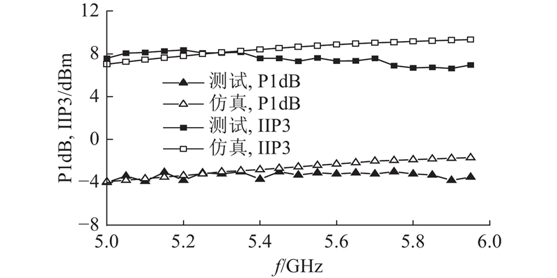
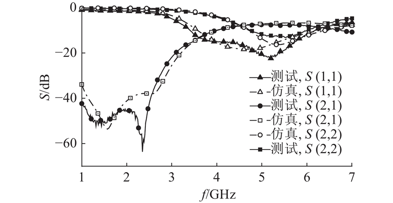
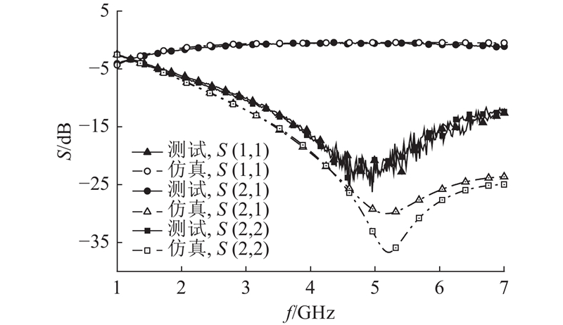
To meet the requirements for high linearity and out-of-band signal suppression in the RF communication front-end receiver, an RF receiver front-end operated at 5-6 GHz based on 130 nm SoI technology was proposed. The RF receiver front-end consisted of a low-noise amplifier (LNA) with bypass and out-of-band suppression, an RF switch, and a bandgap reference bias circuit. For a cascode-based LNA, an LC notch filter was used for input matching to achieve out-of-band suppression. In the bias circuit, a bandgap reference current source was used for temperature compensation for the bias of the LNA, thereby shielding the effect of the power supply ripple. The RF receiver front-end was processed and tested. Results showed that within the operating frequency band of 5–6 GHz, the gain of the receiver chip was 13.4?14.0 dB, input and output reflection coefficients were below ?10 dB, the minimum noise figure was 1.6 dB, the input 1 dB compression point was greater than ?4 dBm, and the input third-order intercept point was greater than +7 dBm. The amplifier was unconditionally stable across the entire frequency band. The DC power consumption was 30 mW at 2 V supply voltage, and the chip area was 0.56 mm2.
Haipeng FU,Zhiqiang CHENG. 5-6 GHz RF receiver front-end with 1.6 dB minimum noise figure and high out-of-band suppression. Journal of ZheJiang University (Engineering Science), 2024, 58(10): 2192-2198.
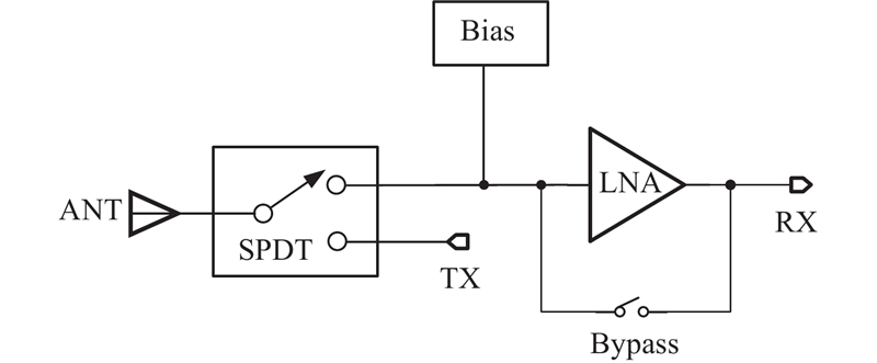
Fig.1Overall block diagram of RF receiver front-end
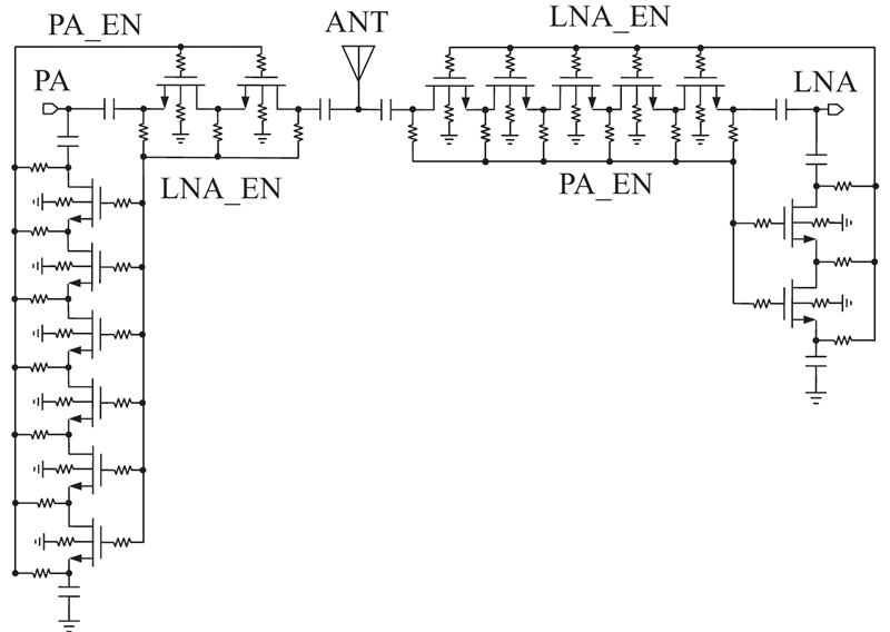
Fig.2RF switch topology
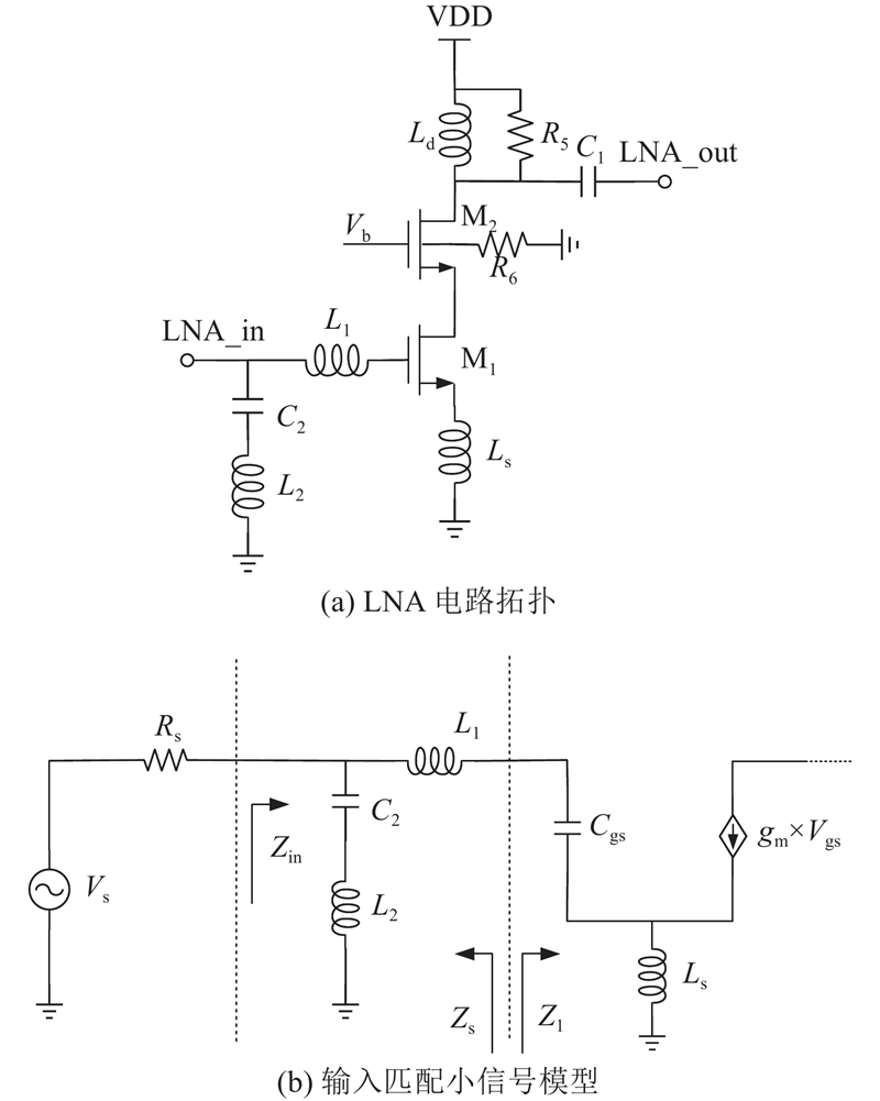
Fig.3LNA topology and input matching small signal model
Fig.4Schematic of low noise amplifier
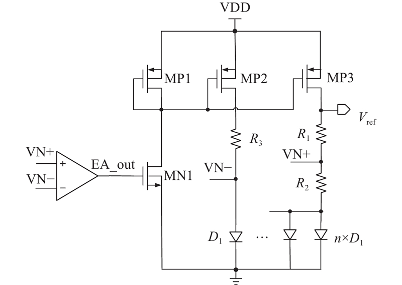
Fig.5Bandgap reference circuit
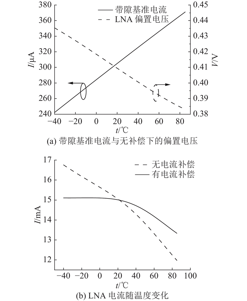
Fig.6Comparison of bias voltage with and without temperature compensation
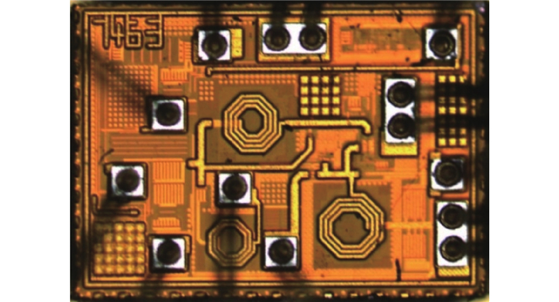
Fig.7Microscopic photo of chip
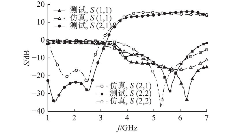
Fig.8Scattering parameter simulation and test results of low noise amplifier
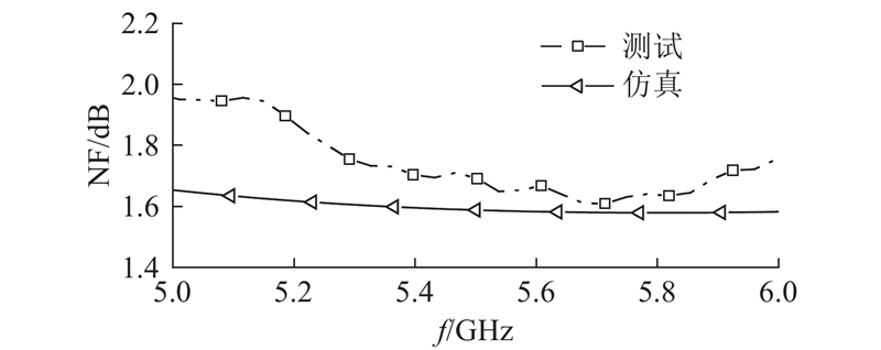
Fig.9Simulation and test results of noise figure
Fig.10Simulation and test results of 1 dB compression point and input third-order intercept point
Fig.11Scattering parameter simulation and test results of bypass
Fig.12Scattering parameter simulation and test results of switch’s PA path
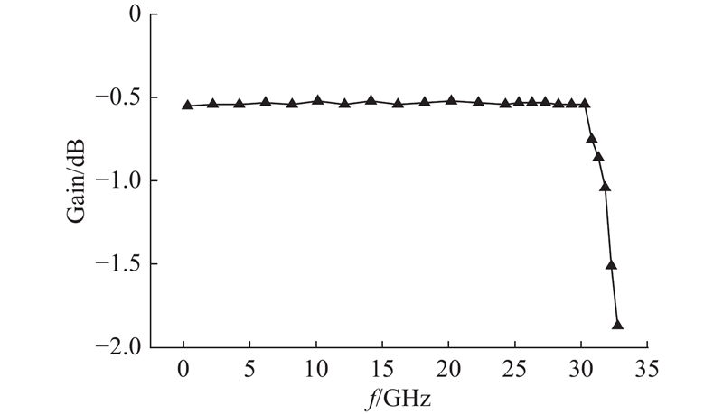
Fig.13Test results of 1 dB compression point for switch’s PA path
工艺
f /GHz
Gainmax/dB
NFmin/dB
IP1dB/dBm
IIP3/dBm
P/mW
A/mm2
FoM/GHz
180 nm CMOS[21]
0.1~2.0
17.5
2.9
?3.00
10.6
21.3
0.63
1.39
180 nm SoI[22]
1.0
10.7
1.3
3.00
22.0
50.0
0.67
1.34
GaAs pHEMT[23]
5.0~6.0
27.0
1.3
?13.00
—
240.0
4.29
1.64
130 nm CMOS[24]
5.0
25.5
1.9
?25.07
0
20.9
1.26
0.48
130 nm SoI(本研究)
5.0~6.0
14.0
1.6
?4.00
7.0
30.0
0.56
4.11
Tab.1Performance comparison of different low noise amplifiers
[1]
SHIRMOHAMMADI B, YAVARI M A linear wideband CMOS balun-LNA with balanced loads[J]. IEEE Transactions on Circuits and Systems II: Express Briefs, 2022, 69 (3): 754- 758
[2]
PANG D, GUI Y, WU S, et al. An ultra-wideband low noise amplifier design in 0.13-um CMOS technology [C]// 2021 IEEE International Conference on Integrated Circuits, Technologies and Applications . Zhuhai: IEEE, 2021: 43–44.
[3]
MUSTAPHA A A, GAYA S, MOHAMMAD B, et al. Wideband low noise amplifiers for mm-wave 5G application using capacitive feedback technique in 22nm FDSOI [C]// 2021 28th IEEE International Conference on Electronics, Circuits, and Systems . Dubai: IEEE, 2021.
[4]
BOZORG A, STASZEWSKI R B A 0.02–4.5-GHz LN(T)A in 28-nm CMOS for 5G exploiting noise reduction and current reuse[J]. IEEE Journal of Solid-State Circuits, 2021, 56 (2): 404- 415
doi: 10.1109/JSSC.2020.3018680
[5]
胡锦, 翟媛, 郝明丽, 等 应用于WLAN的SiGe射频功率放大器的设计[J]. 湖南大学学报: 自然科学版, 2012, 39 (10): 56- 59 HU Jin, ZHAI Yuan, HAO Mingli, et al Design of SiGe RF power amplifier for WLAN[J]. Journal of Hunan University: Natural Sciences, 2012, 39 (10): 56- 59
[6]
LI C, WANG X, JAIN V, et al. 2.4/5.5GHz LNA switch designs based on high resistive substrate 0.35 μm SiGe BiCMOS [C]// 2015 IEEE 11th International Conference on ASIC . Chengdu: IEEE, 2015: 1–4.
[7]
ZOU T, XU H, WANG Y, et al. A capacitor assisting triple-winding transformer low-noise amplifier with 0.8-1.5dB NF 6-12GHz BW ±0.75dB Ripple in 130nm SOI CMOS [C]// 2022 IEEE Radio Frequency Integrated Circuits Symposium . Denver: IEEE, 2022: 231–234.
[8]
PARAT D, SERHAN A, REYNIER P, et al. A linear high-power reconfigurable SOI-CMOS front-end module for WI-FI 6/6E applications [C]// 2022 IEEE Radio Frequency Integrated Circuits Symposium . Denver: IEEE, 2022: 39–42.
[9]
NYSSENS L, RACK M, WANE S, et al. A 2.5-2.6 dB noise figure LNA for 39 GHz band in 22 nm FD-SOI with back-gate bias tunability [C]// 2022 17th European Microwave Integrated Circuits Conference . Milan: IEEE, 2022: 60–63.
[10]
GAO H, SHI J, LIN F. A wideband LNA with gm-boosted and noise cancel technique [C]// 2020 IEEE International Conference on Integrated Circuits, Technologies and Applications . Nanjing: IEEE, 2020: 17–18.
[11]
SHAMS N, KAKHKI A P, NABKI F. Reconfigurable IR-UWB current mode switched receiver for IoT applications [C]// 2019 26th IEEE International Conference on Electronics, Circuits and Systems . Genoa: IEEE, 2019: 9–12.
[12]
曾志, 李远鹏, 陈长友 具有带外抑制特性的Ka波段低功耗低噪声放大器[J]. 半导体技术, 2021, 46 (1): 36- 40 ZENG Zhi, LI Yuanpeng, CHEN Changyou Ka-band low power consumption and low noise amplifier with out-of-band suppression characteristic[J]. Semiconductor Technology, 2021, 46 (1): 36- 40
[13]
ZHANG J, ZHAO D, YOU X Analysis and design of a CMOS LNA with transformer-based integrated notch filter for Ku-band satellite communications[J]. IEEE Transactions on Microwave Theory and Techniques, 2022, 70 (1): 790- 800
doi: 10.1109/TMTT.2021.3126858
[14]
LEE D, KWON K CMOS channel-selection LNA with a feedforward N-path filter and calibrated blocker cancellation path for FEM-less cellular transceivers[J]. IEEE Transactions on Microwave Theory and Techniques, 2022, 70 (3): 1810- 1820
doi: 10.1109/TMTT.2022.3142140
[15]
余巨臣, 彭龙新, 刘昊, 等 具有带外抑制的限幅低噪声放大器一体化设计[J]. 半导体技术, 2022, 47 (6): 493- 497 YU Juchen, PENG Longxin, LIU Hao, et al Integrated design of limiter low noise amplifier with out-of-band rejection[J]. Semiconductor Technology, 2022, 47 (6): 493- 497
[16]
MALEK M I, SAINI S. Improved two stage ultra-wideband CMOS low noise amplifier with out band rejection using low noise active inductor [C]// 2015 International Conference on Signal Processing and Communication Engineering Systems . Guntur: IEEE, 2015: 157–161.
[17]
LI Y, LI X, HUANG Z, et al A novel low-power notch-enhanced active filter for ultrawideband interferer rejected LNA[J]. IEEE Transactions on Microwave Theory and Techniques, 2021, 69 (3): 1684- 1697
doi: 10.1109/TMTT.2021.3053264
[18]
KWON K, KIM S, SON K Y A hybrid transformer-based CMOS duplexer with a single-ended notch-filtered LNA for highly integrated tunable RF front-ends[J]. IEEE Microwave and Wireless Components Letters, 2018, 28 (11): 1032- 1034
doi: 10.1109/LMWC.2018.2869302
NGUYEN T K, OH N J, CHOI H C, et al. CMOS low noise amplifier design optimization technique [C]// The 2004 47th Midwest Symposium on Circuits and Systems . Hiroshima: IEEE, 2004.
[21]
KIM B K, IM D, CHOI J, et al A highly linear 1 GHz 1.3 dB NF CMOS low-noise amplifier with complementary transconductance linearization[J]. IEEE Journal of Solid-State Circuits, 2014, 49 (6): 1286- 1302
doi: 10.1109/JSSC.2014.2319262
[22]
GUO B, CHEN J, LI L, et al A wideband noise-canceling CMOS LNA with enhanced linearity by using complementary nMOS and pMOS configurations[J]. IEEE Journal of Solid-State Circuits, 2017, 52 (5): 1331- 1344
doi: 10.1109/JSSC.2017.2657598
[23]
倪冬欣, 彭龙新, 李建平, 等 5~6 GHz限幅低噪声放大器的研制[J]. 固体电子学研究与进展, 2020, 40 (1): 18- 22 NI Dongxin, PENG Longxin, LI Jianping, et al Development of a 5~6 GHz limiter low noise amplifier[J]. Research and Progress of SSE, 2020, 40 (1): 18- 22