|
|
|
| Low-power and high-efficiency transmitter based on dual-supply voltage and frequency multiplication technique |
Meng-qian CUI1( ),Pei-sheng ZONG2,Guo WEI1,Ke-ping WANG1,*() ),Pei-sheng ZONG2,Guo WEI1,Ke-ping WANG1,*() |
1. School of Microelectronic, Tianjin University, Tianjin 300072, China
2. School of Information Science and Engineering, Southeast University, Nanjing 211189, China |
|
|
|
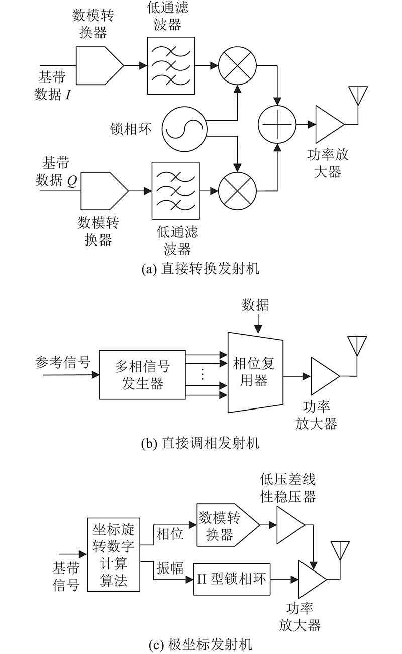
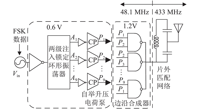
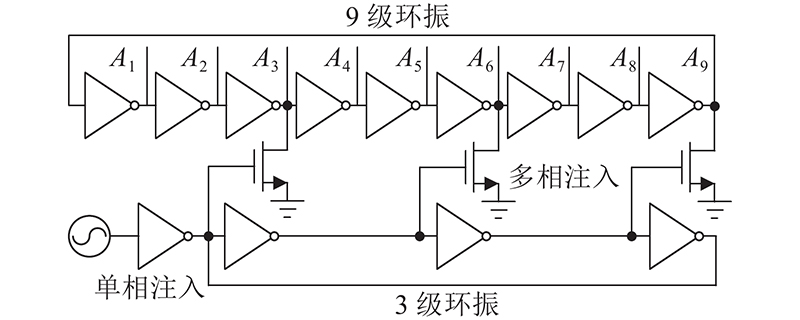
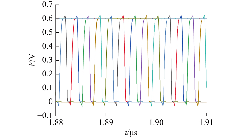
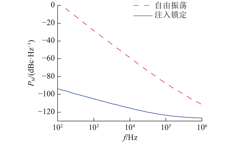
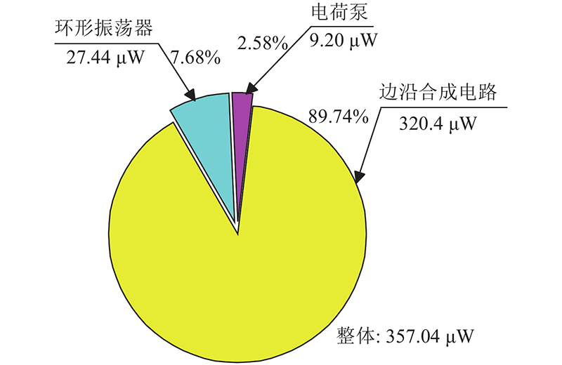
Abstract A new transmitter architecture was proposed to solve the high power consumption and low efficiency problems of the traditional transmitter in order to overcome the limitation of battery capacity and prolong the standby time of the chip. A two-stage ring oscillator based on injection locking technique was used to provide multiphase signal. The self-boosted charge pump circuit boosts the voltage of the multi-phase signal in order to achieve a low-voltage and low-power design. The edge combiner was used to multiply the frequency of the multiphase signal, which ensured that the pre-stage circuit can work at low frequency with low power consumption. The 433 MHz ISM transmitter was designed in a 55 nm CMOS technique for verification. The simulation results show that the output power is ?9.7 dBm. The ring oscillator and charge pump can work at a 0.6 V supply, and the edge combiner works under 1.2 V supply. The whole transmitter consumes 357.04 μW, the efficiency is 29.83%, and the layout occupies an area of 70 μm×100 μm. The simulation results show that the proposed structure has the advantages of low power consumption, high efficiency, small area and low complexity.
|
|
Received: 29 June 2021
Published: 26 July 2022
|
|
|
| Fund: 国家自然科学基金资助项目(61774035);江苏省自然科学基金资助项目(BK20191260) |
|
Corresponding Authors:
Ke-ping WANG
E-mail: cmq_15028576218@sina.com;kpwang@tju.edu.cn
|
基于双电压和倍频技术的低功耗高效率发射机
为了克服电池容量的局限性,延长芯片的待机时间,针对传统发射机的高功耗、低效率问题,提出新型发射机架构. 采用2级注入锁定环形振荡器提供多相信号,电荷泵自举升压电路对该多相信号进行电压提升,实现低电压低功耗设计. 边沿合成器对多相信号进行倍频,使前级电路工作在低频,降低系统功耗. 基于55 nm CMOS工艺,设计433 MHz ISM频段发射机进行验证. 仿真结果表明,发射机的输出功率为?9.7 dBm,环形振荡器和电荷泵自举升压电路工作在0.6 V电源电压下,边沿合成器工作在1.2 V电源电压下,发射机整体功耗为357.04 μW,效率为29.83%,版图面积为70 μm×100 μm. 实验结果证明,所提结构具有功耗低、效率高、面积小和复杂度低的优点.
关键词:
发射机,
低功耗,
低电压,
自举升压,
边沿合成,
注入锁定
|
|
| [1] |
LEE M C, KARIMI-BIDHENDI A, MALEKZADEH-ARASTEH O, et al. A CMOS inductorless MedRadio OOK transceiver with a 42μW event-driven supply-modulated RX and a 14% efficiency TX for medical implants [C]// 2018 IEEE Custom Integrated Circuits Conference. San Diego: IEEE, 2018: 1-4.
|
|
|
| [2] |
YUN S J, LEE J, KANG J, et al. A low power fully integrated RF transceiver for medical implant communication [C]// 2018 IEEE International Symposium on Circuits and Systems. Florence: IEEE, 2018: 1-4.
|
|
|
| [3] |
WANG K P, QIU L, KOO J, et al Design of 1.8-mW PLL-free 2.4-GHz receiver utilizing temperature-compensated FBAR resonator[J]. IEEE Journal of Solid-State Circuits, 2018, 53 (6): 1628- 1639
doi: 10.1109/JSSC.2018.2801829
|
|
|
| [4] |
WANG K P, OTIS B, WANG Z G A 580-μW 2.4-GHz ZigBee receiver front end with transformer coupling technique[J]. IEEE Microwave and Wireless Components Letters, 2018, 28 (2): 174- 176
doi: 10.1109/LMWC.2017.2787064
|
|
|
| [5] |
RAI S, HOLLEMAN J, PANDEY J N, et al. A 500µW neural tag with 2µVrms AFE and frequency-multiplying MICS/ISM FSK transmitter [C]// 2009 IEEE International Solid-State Circuits Conference: Digest of Technical Papers. San Francisco: IEEE, 2009: 212-213.
|
|
|
| [6] |
王曾祺. WSN低功耗射频接收关键技术研究与芯片设计[D]. 南京: 东南大学, 2017.
WANG Zeng-qi. Low power RF receiver key technologies research and chip design for wireless sensor network applications [D]. Nanjing: Southeast University, 2017.
|
|
|
| [7] |
周于浩. 基于注入锁定和倍频的低功耗发射机芯片设计[D]. 南京: 东南大学, 2019.
ZHOU Yu-hao. Design of a low-power transmitter based on injection-locking and frequency multiplication [D]. Nanjing: Southeast University, 2019.
|
|
|
| [8] |
PANDEY J, OTIS B P A sub-100 μW MICS/ISM band transmitter based on injection-locking and frequency multiplication[J]. IEEE Journal of Solid-State Circuits, 2011, 46 (5): 1049- 1058
doi: 10.1109/JSSC.2011.2118030
|
|
|
| [9] |
JAHAN M S, LANGFORD J, HOLLEMAN J. A low-power FSK/OOK transmitter for 915 MHz ISM band [C]// 2015 IEEE Radio Frequency Integrated Circuits Symposium. Phoenix: IEEE, 2015: 163-166.
|
|
|
| [10] |
DIAO S X, ZHENG Y J, GAO Y, et al A 50-Mb/s CMOS QPSK/O-QPSK transmitter employing injection locking for direct modulation[J]. IEEE Transactions on Microwave Theory and Techniques, 2012, 60 (1): 120- 130
doi: 10.1109/TMTT.2011.2174377
|
|
|
| [11] |
IZAD M M, HENG C H. A 17pJ/bit 915MHz 8PSK/O-QPSK transmitter for high data rate biomedical applications [C]// Proceedings of the IEEE 2012 Custom Integrated Circuits Conference. San Jose: IEEE, 2012: 1-4.
|
|
|
| [12] |
DAU N, CHEN Y T, LIAO Y T. A 145μW 315MHz harmonically injection-locked RF transmitter with two-step frequency multiplication techniques [C]// 2017 IEEE MTT-S International Microwave Symposium. Honololu: IEEE, 2017: 1781-1783.
|
|
|
| [13] |
GUO Y G, MAI S P, WENG Z Y, et al. A 9.4 pJ/bit 432 MHz 16-QAM/MSK transmitter based on edge-combining power amplifier [C]// 2017 IEEE International Symposium on Circuits and Systems. Baltimore: IEEE, 2017: 1-4.
|
|
|
| [14] |
TSAI Y L, LIN C Y, WANG B C, et al A 330-μW 400-MHz BPSK transmitter in 0.18-μm CMOS for biomedical applications[J]. IEEE Transactions on Circuits and Systems II: Express Briefs, 2016, 63 (5): 448- 452
doi: 10.1109/TCSII.2015.2505080
|
|
|
| [15] |
ZHOU Y S, YUAN F A study of the lock range of injection-locked CMOS active-inductor oscillators using a linear control system approach[J]. IEEE Transactions on Circuits and Systems II: Express Briefs, 2011, 58 (10): 627- 631
doi: 10.1109/TCSII.2011.2164154
|
|
|
| [16] |
KER M D, CHEN S L, TSAI C S Design of charge pump circuit with consideration of gate-oxide reliability in low-voltage CMOS processes[J]. IEEE Journal of Solid-State Circuits, 2006, 45 (5): 1100- 1107
|
|
|
| [17] |
TANZAWA T, TANAKA T A dynamic analysis of the Dickson charge pump circuit[J]. IEEE Journal of Solid-State Circuits, 1997, 32 (8): 1231- 1240
doi: 10.1109/4.604079
|
|
|
| [18] |
DICKSON J F On-chip high-voltage generation in MNOS integrated circuits using an improved voltage multiplier technique[J]. IEEE Journal of Solid-State Circuits, 1976, 11 (3): 374- 378
doi: 10.1109/JSSC.1976.1050739
|
|
|
| [19] |
ZHOU Y X, WANG Z H, WANG K P. High-efficiency charge pumps with no reversion loss by utilizing gate voltage boosting technique [C]// 2020 IEEE International Symposium on Circuits and Systems. Seville: IEEE, 2020: 1-5.
|
|
|
| [20] |
JIANG T Q, YIN J, MAK P I, et al A 0.5-V 0.4-to-1.6-GHz 8-phase bootstrap ring-VCO using Inherent non-overlapping clocks achieving a 162.2-dBc/Hz FoM[J]. IEEE Transactions on Circuits and Systems II: Express Briefs, 2019, 66 (2): 157- 161
doi: 10.1109/TCSII.2018.2842185
|
|
|
| [21] |
CHEN X, BREIHOLZ J, YAHYA F B, et al Analysis and design of an ultra-low-power bluetooth low-energy transmitter with ring oscillator-based ADPLL and 4× frequency edge combiner[J]. IEEE Journal of Solid-State Circuits, 2019, 54 (5): 1339- 1350
doi: 10.1109/JSSC.2019.2896404
|
|
|
| [22] |
CHUANG C N, LIU S L A 3–8 GHz delay-locked loop with cycle jitter calibration[J]. IEEE Transactions on Circuits and Systems II: Express Briefs, 2008, 55 (11): 1094- 1098
doi: 10.1109/TCSII.2008.2002561
|
|
|
| [23] |
WENG Z Y, JIANG H J, GUO Y S, et al. A 400MHz/900MHz dual-band ultra-low-power digital transmitter for biomedical applications [C]// 2020 IEEE Radio Frequency Integrated Circuits Symposium. Los Angeles: IEEE, 2020: 331-334.
|
|
|
| [24] |
LIN C C, HU H, GUPTA S. A 66.97pJ/bit, 0.0413mm2 self-aligned PLL-calibrated harmonic-injection-locked TX with > 62dBc spur suppression for IoT applications [C]// 2020 IEEE Radio Frequency Integrated Circuits Symposium. Los Angeles: IEEE, 2020: 323-326.
|
|
|
|
Viewed |
|
|
|
Full text
|
|
|
|
|
Abstract
|
|
|
|
|
Cited |
|
|
|
|
| |
Shared |
|
|
|
|
| |
Discussed |
|
|
|
|