| 机械设计理论与方法 |
|


|
|
|
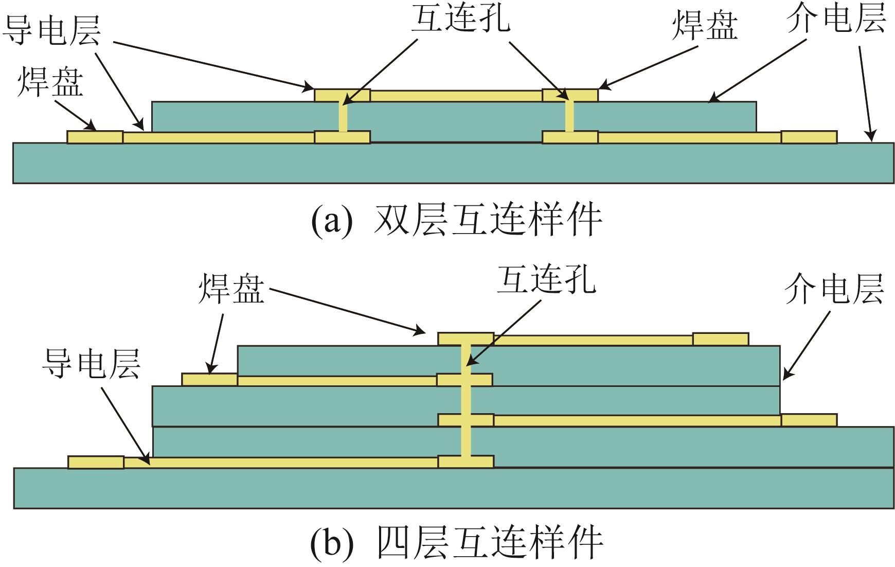
| 基于压电喷墨打印技术的多层电路垂直互连工艺研究 |
林枝城1( ),加泽贤1,苟宁2,孙岩辉1(),吕景祥1,尹恩怀2,李超2 ),加泽贤1,苟宁2,孙岩辉1(),吕景祥1,尹恩怀2,李超2 |
1.长安大学 道路施工技术与装备教育部重点实验室,陕西 西安 710064
2.西安瑞特三维科技有限公司,陕西 西安 710068 |
|
| Research on vertical interconnect process of multilayer circuits based on piezoelectric inkjet printing technology |
| Zhicheng LIN1(),Zexian JIA1,Ning GOU2,Yanhui SUN1(),Jingxiang Lü1,Enhuai YIN2,Chao LI2 |
1.Key Laboratory of Road Construction Technology and Equipment of Ministry of Education, Chang'an University, Xi'an 710064, China
2.Xi'an Ruite 3D Technology Co. , Ltd. , Xi'an 710068, China |
引用本文:
林枝城,加泽贤,苟宁,孙岩辉,吕景祥,尹恩怀,李超. 基于压电喷墨打印技术的多层电路垂直互连工艺研究[J]. 工程设计学报, 2025, 32(6): 780-788.
Zhicheng LIN,Zexian JIA,Ning GOU,Yanhui SUN,Jingxiang Lü,Enhuai YIN,Chao LI. Research on vertical interconnect process of multilayer circuits based on piezoelectric inkjet printing technology[J]. Chinese Journal of Engineering Design, 2025, 32(6): 780-788.
链接本文:
https://www.zjujournals.com/gcsjxb/CN/10.3785/j.issn.1006-754X.2025.05.131
或
https://www.zjujournals.com/gcsjxb/CN/Y2025/V32/I6/780
|
| [1] |
GARICH H, GEBHART L, TAYLOR E J, et al. Development and characterization of plating cell geometry for PCB and packaging applications[J]. ECS Transactions, 2007, 3(16): 1-10.
|
| [2] |
JI L N, GONG Y, YANG Z G. Failure investigation on copper-plated blind vias in PCB[J]. Microelectronics Reliability, 2010, 50(8): 1163-1170.
|
| [3] |
BERNHARD T, BRANAGAN S, SCHULZ R, et al. The formation of nano-voids in electroless Cu layers[J]. MRS Advances, 2019, 4(41/42): 2231-2240.
|
| [4] |
NASSAJFAR M N, DEVIATKIN I, LEMINEN V, et al. Alternative materials for printed circuit board production: an environmental perspective[J]. Sustainability, 2021, 13(21): 12126.
|
| [5] |
TAN H W, CHOONG Y Y C, KUO C N, et al. 3D printed electronics: processes, materials and future trends[J]. Progress in Materials Science, 2022, 127: 100945.
|
| [6] |
沈诚, 邹平, 康迪, 等. 超声振动透镜辅助激光打孔实验研究[J]. 中国机械工程, 2020, 31(21): 2542-2546.
SHEN C, ZOU P, KANG D, et al. Experimental study on ultrasonic vibration lens assisted laser drilling[J]. China Mechanical Engineering, 2020, 31(21): 2542-2546.
|
| [7] |
李志明, 王玺, 聂劲松. 飞秒激光打孔硅的孔洞形貌研究[J]. 光子学报, 2017, 46(10): 29-36. doi:10.3788/gzxb20174610.1014004
LI Z M, WANG X, NIE J S. Hole morphology in femtosecond laser drilling of silicon[J]. Acta Photonica Sinica, 2017, 46(10): 29-36.
doi: 10.3788/gzxb20174610.1014004
|
| [8] |
ALWAIDH A, SHARP M, FRENCH P. Laser processing of rigid and flexible PCBs[J]. Optics and Lasers in Engineering, 2014, 58: 109-113.
|
| [9] |
DING C F, LEE M S, LI K M. Low-cost camera based laser power monitoring and stabilizing for micro-hole drilling[J]. International Journal of Precision Engineering and Manufacturing, 2017, 18(9): 1205-1212.
|
| [10] |
LO T M, YOUNG J S. Improvements of productivity for PCB drilling by laser driller machine[J]. International Journal of Precision Engineering and Manufacturing, 2014, 15(8): 1575-1581.
|
| [11] |
LEE D. Picosecond IR pulsed laser drilling of copper-coated glass/epoxy composite[J]. IEEE Transactions on Components, Packaging and Manufacturing Technology, 2017, 7(12): 2066-2072.
|
| [12] |
牟娟, 陈燕, 徐九华, 等. 钎焊套料钻钻削碳纤维增强复合材料层合板出口撕裂缺陷的成因分析[J]. 中国机械工程, 2013, 24(20): 2699-2704.
MU J, CHEN Y, XU J H, et al. Analysis on cracking at exit of hole drilled in carbon fiber reinforced plastics laminate with brazed diamond core drill[J]. China Mechanical Engineering, 2013, 24(20): 2699-2704.
|
| [13] |
SHI H Y, LIU X W, LOU Y. Materials and micro drilling of high frequency and high speed printed circuit board: a review[J]. The International Journal of Advanced Manufacturing Technology, 2019, 100(1): 827-841.
|
| [14] |
LIN D T, WANG C Y, FU L Y, et al. Cryogenic auxiliary drilling of printed circuit boards[J]. Circuit World, 2019, 45(4): 279-286.
|
| [15] |
XU B, FENG X K, WU X Y, et al. Micro-EDM-assisted machining micro-holes in printed circuit board[J]. The International Journal of Advanced Manufacturing Technology, 2021, 113(3): 1191-1201.
|
| [16] |
ZHENG X H, DONG D P, HUANG L X, et al. Research on fixture hole drilling quality of printed circuit board[J]. International Journal of Precision Engineering and Manufacturing, 2013, 14(4): 525-534.
|
| [17] |
KIM S, SHAMIM A, GEORGIADIS A, et al. Fabrication of fully inkjet-printed vias and SIW structures on thick polymer substrates[J]. IEEE Transactions on Components, Packaging and Manufacturing Technology, 2016, 6(3): 486-496.
|
| [18] |
KHORRAMDEL B, MäNTYSALO M. Fabrication and electrical characterization of partially metallized vias fabricated by inkjet[J]. Journal of Micromechanics and Microengineering, 2016, 26(4): 045017.
|
| [19] |
BACH H L, YU Z C, LETZ S, et al. Vias in DBC substrates for embedded power modules[C]//10th International Conference on Integrated Power Electronics Systems. Stuttgart, Mar. 20-22, 2018.
|
| [20] |
CHEN S T, CHENG Y S, CHANG Y H, et al. Activation of amino-based monolayers for electroless metallization of high-aspect-ratio through-silicon vias by using a simple ultrasonic-assisted plating solution[J]. Applied Surface Science, 2018, 440: 209-216.
|
| [21] |
C. H R, KOTHURU A, SINGH A P, et al. Plasma treatment and copper metallization for reliable plated-through-holes in microwave PCBs for space electronic packaging[J]. IEEE Transactions on Components, Packaging and Manufacturing Technology, 2020, 10(11): 1921-1928.
|
| [22] |
GRIGORYAN N S, SAVITSKAYA S A, ASNIS N A, et al. Surface preparation before chemical copper plating of holes in printed circuit boards. Part I[J]. International Journal of Corrosion and Scale Inhibition, 2022, 11(4): 1593-1603.
|
| [23] |
XIANG J, WANG C, CHEN Y M, et al. Numerical simulation and experiments to improve throwing power for practical PCB through-holes plating[J]. Circuit World, 2019, 45(4): 221-230.
|
|
Viewed |
|
|
|
Full text
|
|
|
|
|
Abstract
|
|
|
|
|
Cited |
|
|
|
|
| |
Shared |
|
|
|
|
| |
Discussed |
|
|
|
|