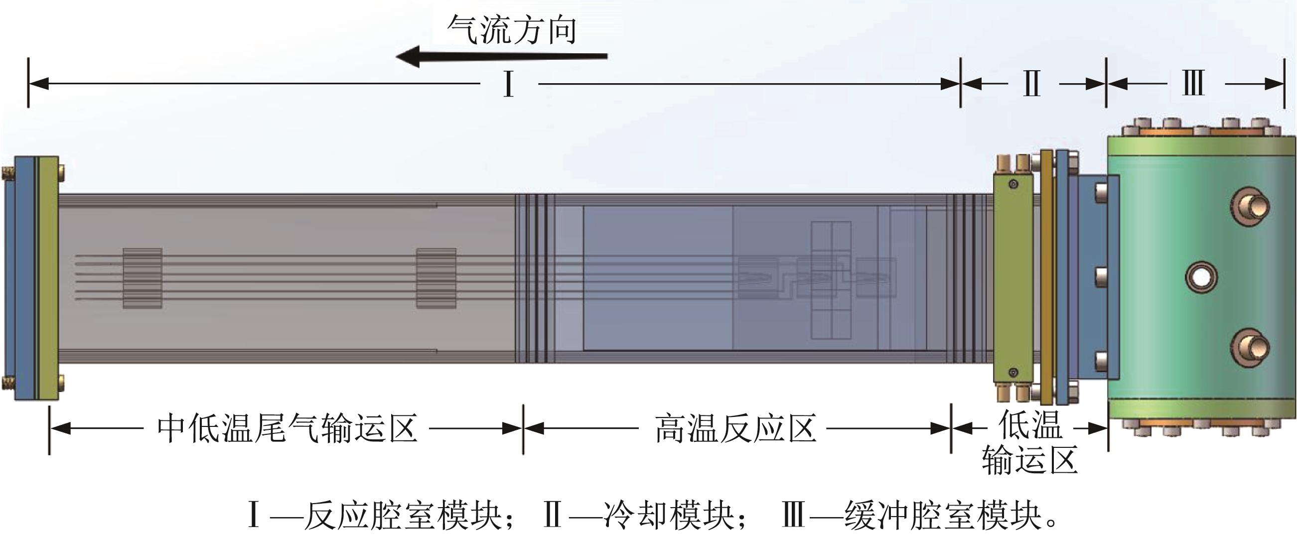
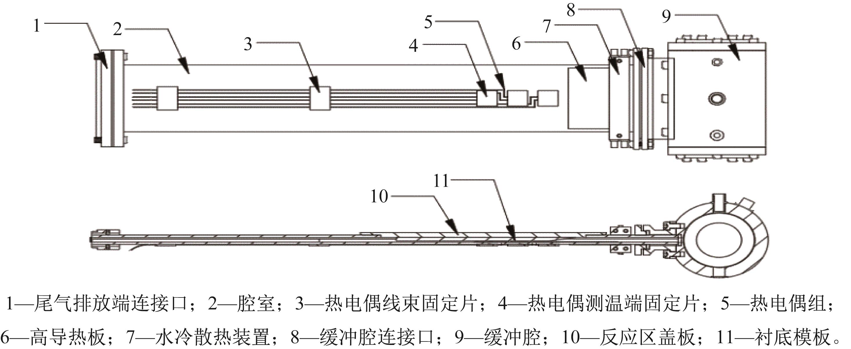
|
|
| [1] |
胡昌义,李靖华.化学气相沉积技术与材料制备[J].稀有金属,2001,25(5):5.
HU C Y, LI J H. Chemical vapor deposition and preparation of materials[J]. Chinese Journal of Rare Metals, 2001, 25(5): 5.
|
|
|
| [2] |
任文才,高力波,马来鹏,等.石墨烯的化学气相沉积法制备[J].新型炭材料,2011,26(1):71-80.
REN W C, GAO L B, MA L P, et al. Preparation of graphene by chemical vapor deposition[J]. New Carbon Materials, 2011, 26(1): 71-80.
|
|
|
| [3] |
蒋运才,曹昌蝶,刘岚君,等.化学气相沉积法制备二维材料研究进展[J].化工新型材料,2021,49(11):59-62.
JIANG Y C, CAO C D, LIU L J, et al. Progress in the preparation of two-dimensional materials by chemical vapor deposition[J]. New Chemical Materials, 2021, 49(11): 59-62.
|
|
|
| [4] |
庞世红,王承遇,马眷荣,等.常压化学气相沉积法制备二氧化钛薄膜的沉积工艺及薄膜均匀性[J].硅酸盐学报,2010,38(1):64-67.
PANG S H, WANG C Y, MA J R, et al. Deposition process and uniformity of titanium dioxide film prepared by atmosphere chemical vapor deposition[J]. Journal of the Chinese Ceramic Society, 2010, 38(1): 64-67.
|
|
|
| [5] |
王汐璆,庄文昌,张凯惠,等.化学气相沉积法制备氧化镓纳米线[J].人工晶体学报,2019,48(12):2174-2178. doi:10.3969/j.issn.1000-985X.2019.12.002
WANG X Q, ZHUANG W C, ZHANG K H, et al. Preparation of gallium oxide nanowires by chemical vapor deposition[J]. Journal of Artificial Crystals, 2019, 48(12): 2174-2178.
doi: 10.3969/j.issn.1000-985X.2019.12.002
|
|
|
| [6] |
PARK S Y, HA M T, KIM K H, et al. Enhanced thickness uniformity of large-scale α-Ga2O3 epilayers grown by vertical hot-wall mist chemical vapor deposition[J]. Ceramics International, 2022, 48(4): 5075-5082.
|
|
|
| [7] |
HYEON K S, MINO Y, LEE H Y, et al. Structural characteristics of α-Ga2O3 films grown on sapphire by halide vapor phase epitaxy[J]. Materials Science in Semiconductor Processing, 2021, 123: 1-4.
|
|
|
| [8] |
JINNO R, YOSHIMURA N, KANEKO K, et al. Enhancement of epitaxial lateral overgrowth in the mist chemical vapor deposition of α-Ga2O3 by using a-plane sapphire substrate[J]. Japanese Journal of Applied Physics, 2019, 58(12): 9-12.
|
|
|
| [9] |
XU Y, ZHANG C F, CHENG Y L, et al. Influence of carrier gases on the quality of epitaxial corundum-structured α-Ga2O3 films grown by mist chemical vapor deposition method[J]. Materials, 2019, 12(22): 3670-3671.
|
|
|
| [10] |
SON H K, CHOI Y J, HA J S, et al. Crystal quality improvement of α-Ga2O3 growth on stripe patterned template via epitaxial lateral overgrowth[J]. Crystal Growth and Design, 2019, 19(9): 5105-5110.
|
|
|
| [11] |
CHENG Y L, XU Y, LI Z, et al. Heteroepitaxial growth of α-Ga2O3 thin films on a-, c- and r-plane sapphire substrates by low-cost mist-CVD method[J]. Journal of Alloys and Compounds, 2020, 831: 1-3.
|
|
|
| [12] |
LEILA G, JACQUELINE C, GIANG T D, et al. Optical characterization of gallium oxide α and β Polymorph thin-films grown on c-plane sapphire[J]. Journal of Electronic Materials, 2021, 50(6): 2990-2998.
|
|
|
| [13] |
龚恒翔,冯倩,郝跃,等.雾化辅助CVD薄膜沉积方法:CN109440083B[P]. 2020-09-25.
GONG H X, FENG Q, HAO Y, et al. Atomization-assisted CVD thin film deposition method: CN109440083B[P]. 2020-09-25.
|
|
|
| [14] |
王超,孙文旭,马晓静,等.基于模糊控制的HVPE生长设备温度控制系统[J].工程设计学报,2020,27(6):765-770. doi:10.3785/j.issn.1006-754X.2020.00.083
WANG C, SUN W X, MA X J, et al. Temperature control system of HVPE growth equipment based on fuzzy control[J]. Chinese Journal of Engineering Design, 2020, 27(6):765-770.
doi: 10.3785/j.issn.1006-754X.2020.00.083
|
|
|
| [15] |
孙华.一种反应室及CVD沉积石墨烯的规模化制备设备:CN215249591U[P].2021-12-21.
SUN H. A reaction chamber and scale-up preparation equipment for CVD deposition of graphene: CN215249591U[P]. 2021-12-21.
|
|
|
| [16] |
于伟华,朱建中,鞠德胜,等.一种用于CVD反应器的喷嘴装置及CVD反应器:CN215757598U[P].2022-02-08.
YU W H, ZHU J Z, JU D S, et al. A nozzle device for CVD reactor and CVD reactor: CN215757598U[P]. 2022-02-08.
|
|
|
| [17] |
宋德鹏,陈占领.CVD真空设备及立卧切换实现方法:CN114086153A[P].2022-02-25.
SONG D P, CHEN Z L. CVD vacuum equipment and vertical and horizontal switching implementation method: CN114086153A[P]. 2022-02-25.
|
|
|
| [18] |
黄大凯.一种实施气相沉积法工艺的高速清洁的CVD腔室结构:CN113930747A[P].2022-01-14.
HUANG D K. A high-speed clean CVD chamber structure for implementing vapor deposition method process: CN113930747A[P]. 2022-01-14.
|
|
|
| [19] |
陈欣.紧耦合气雾化流场结构和雾化机理研究[D].长沙:中南大学,2007:1-97.
CHEN X. Study on the structure and atomization mechanism of tightly coupled aerosolized flow field[D]. Changsha: Central South University, 2007: 1-97.
|
|
|
| [20] |
刘宏明,林琳.一种改善气体分布的CVD金刚石生长设备:CN216377494U[P].2022-04-26.
LIU H M, LIN L. A CVD diamond growth device with improved gas distribution: CN216377494U [P]. 2022-04-26.
|
|
|
| [21] |
黎波,龚恒翔,孟祥杰,等.超声喷雾热分解法制备 ZnO 薄膜及衬底温度对其性能的影响[J]. 人工晶体学报,2014, 43(3):523-527.
LI B, GONG H X, MENG X J, et al. Influence of substrate temperature on the performance of ZnO thin films prepared by ultrosonic spray pyrolysis method[J]. Journal of Synthetic Crystals, 2014, 43(3): 523-527.
|
|
|
| [22] |
马同川.亚稳相氧化镓Mist-CVD异质外延研究[D].南京:南京大学,2020:10-11. doi:10.26478/ja2019.7.11.1
MA T C. Sub-stable phase Ga2O3 Mist-CVD heterogeneous epitaxy study[D]. Nanjing: Nanjing University, 2020:10-11.
doi: 10.26478/ja2019.7.11.1
|
|
|
| [23] |
张志海.喷雾热解法制备氟掺杂二氧化锡导电薄膜及其性能研究[D].合肥:合肥工业大学, 2010:1-75.
ZHANG Z H. Preparation and properties of fluorine doped tin dioxide conductive films by spray pyrolysis[D]. Hefei: Hefei University of Technology, 2010: 1-75.
|
|
|